Display apparatus

a technology of display apparatus and display screen, which is applied in the field of display screen, can solve the problems of deteriorating positioning accuracy of step exposure using a stepper, circuits on the support substrate are more likely to be affected, and circuits on the support substrate are large-scale in terms of layout, so as to achieve the effect of simple calculation, reduced pitch of dots on the smaller-scale circuit side, and increased pitch of dots on the larger-scale circuit sid

Active Publication Date: 2010-12-28
HANNSTAR DISPLAY CORPORATION
View PDF3 Cites 9 Cited by
  • Summary
  • Abstract
  • Description
  • Claims
  • Application Information

AI Technical Summary

Benefits of technology

[0026]An object of the present invention therefore is to provide a display apparatus with built-in circuits, in which the circuit area is decreased. It is another object of the present invention to provide a display apparatus with built-in circuits, in which the size / weight thereof is reduced by decreasing the frame including the circuit part. It is still another object of the present invention to provide a display apparatus with built-in circuits, in which the difficulty of providing layout is decreased. It is yet another object of the present invention to provide a display apparatus that is capable of achieving short TAT and low cost. Furthermore, a further object is to provide a display apparatus with short LT. A still further object of the present invention is to provide a highly fine display apparatus.
[0033]The effects of the present invention will be described. As will be shown in the embodiments, the scale of the circuit provided in the right-and-left direction (lateral direction) of the display part and that of the circuit provided to the top-and-bottom direction (longitudinal direction) of the display part are different. That is, normally, the scale of the circuit provided in the top-and-bottom direction has a larger scale. By forming the dots that correspond to the color layout of the color filters or light-emitting elements into laterally long shapes and by supplying data of a plurality of colors to a single signal line, the pitch of the dots on the larger-scale circuit side can be increased. Meanwhile, the pitch of the dots on the smaller-scale circuit side is decreased. At the same time, the scale of the circuit becomes larger for the number of colors being arranged, since the colors are different by each signal line. In this case, assuming that the number of colors is k, and a ratio of the difference in the circuit scales is q (q is larger than 1), conventionally, the scale of the circuit on the signal line side is “k·q” when the circuit on the scanning line side is 1, and the entire circuit scale is “1+k·q”. With the present invention, however, the scale of the circuit on the scanning line side is k, and that of the circuit on the signal line side is q, so that the entire circuit scale becomes “k+q”. The condition with which the circuit scale of the present invention becomes smaller than that of the conventional structure is “1+k·q>k+q”, and “k>1” can be obtained by a simple calculation. That is, when there are a plurality of colors, the entire circuit scale can be decreased with the present invention. When the scanning line drive circuit is provided in the top-and-bottom direction of the display part, the effects of the present invention can be achieved as well by setting a large dot pitch for the pitch of the large-scaled circuit that is on the side with no scanning line drive circuit, i.e. the dot pitch in the top-and-bottom direction.
[0034]In the display apparatus according to the present invention, the small-scaled first circuit is provided to the outer side of the first direction of the display part, the large-scaled second circuit is provided to the outer side of the second direction of the display part, and the shape of the dot is set to be longer in the first direction and shorter in the second direction. With this, the area of the second circuit per wiring can be taken largely in the first direction, so that the length of the second circuit in the second direction can be shortened. As a result, it is possible to achieve the effect of narrowing the frame.
[0035]In other words, the first effect is that it is possible to provide a display apparatus in which the scale of the entire drive circuit can be drastically reduced by forming the shape of the dots that constitute the pixels into laterally long shapes. The reason for this is that, as will be described in the embodiments, the circuit scales are different between the circuit provided in the right-and-left direction (lateral direction) of the display part and the circuit provided in the top-and-bottom direction (longitudinal direction) of the display part. The present invention is capable of reducing the scale of the entire circuit that is large scaled. Thus, the scale of the entire drive circuit can be drastically reduced. The second effect is that the frame can be decreased by reducing the scale of the circuit that has a larger scale. The third effect is that the development time required for designing / layout can be cut since the scale of the entire drive circuit is reduced, thereby achieving the low cost. The fourth effect is that the present invention is capable of providing a highly reliable display apparatus, in which the provability of generating failures can be decreased because the circuit scale is reduced. The fifth effect is that the frame is reduced, so that the number of display apparatuses fabricated on a single support substrate can be increased (number of products produced therefrom is increased), thereby achieving the low cost. The sixth effect is that the frame is reduced, so that the size and weight of the display apparatus can be reduced. The seventh effect is that the layout of the circuit can be arranged without using an additional wiring layer because the layout of the circuit becomes simple. As a result, it is possible to achieve a drastic cut in the cost in terms of manufacture and design. The eighth effect is that the highly fine display apparatus can be achieved without changing the design rule, since the layout of the circuits can be designed within the range of the circuit pitch based on the design rule. The ninth effect is that the external shape of the display apparatus having a non-rectangular display area can be formed in a shape similar to that of the display area. The reason is that the circuit scale of the peripheral circuits can be formed small and arranged in a well-balanced manner.

Problems solved by technology

The first issue is that the circuits on the support substrate tend to be large-scaled in terms of the layout compared to that of the circuits formed by LSI outside the support substrate.
It is because the size of the support substrate used in the display apparatus is generally larger than that of the silicon substrate used in the LSI technique, so that the circuits on the support substrate are more likely to be affected by expansion / contraction of the support substrate itself, or the positioning accuracy by step exposure using a stepper becomes deteriorated, etc.
The second issue is that it is highly difficult to design the layout of the circuits on the support substrate.
This is due to the fact that it is difficult to decrease the area occupied especially by the circuits on the signal drive circuit side, in addition to the fact that it requires a contrivance to save the occupied area because the design rule mentioned above is large.
This is because the circuits on the signal drive circuit side include not only the scanning circuit but also the analog switch, the level shifter, DAC and the like as described above, so that the circuit structure becomes complicated.
When the pitch in the area for arranging the circuits is narrow, it becomes difficult to draw around the wirings for the input signals necessary for each circuit and the input / output signals between each circuit.
As a result, the difficulty of the circuit layout is increased.
The third issue is that the frame (the distance between the end of the display area and the end face of the support substrate) on the signal drive circuit side becomes increased.
This is caused because the circuit structure on the signal drive circuit side is complicated and the pitch of the layout is narrow, so that the area occupied by the wirings for the signals is increased.
The fourth issue is that it cannot achieve a highly fine display apparatus.
This issue is different from the aforementioned issues concerning expansion of the frame and an increase in the difficulty of layout.
Rather, the issue is that it is not possible to design the layout itself, so the apparatus itself cannot be formed.
For changing the design rule, it is necessary to start from a new process development, which is very difficult.
The fifth issue is that the time required for the development is increased.
The sixth issue is that the cost for the display apparatus is increased.
As described above, this is because the time required for the development is increased, thereby mounting up the development cost.
Further, another reason for this is that it requires a large number of metal layers since providing the layout is highly difficult.
The seventh issue is that an external shape of the display apparatus having a non-rectangular display area becomes largely changed.
However, it is difficult with the conventional display apparatus to make the external shape in a similar shape of the display area.

Method used


Image

  • Display apparatus
  • Display apparatus
  • Display apparatus

Examples


second embodiment

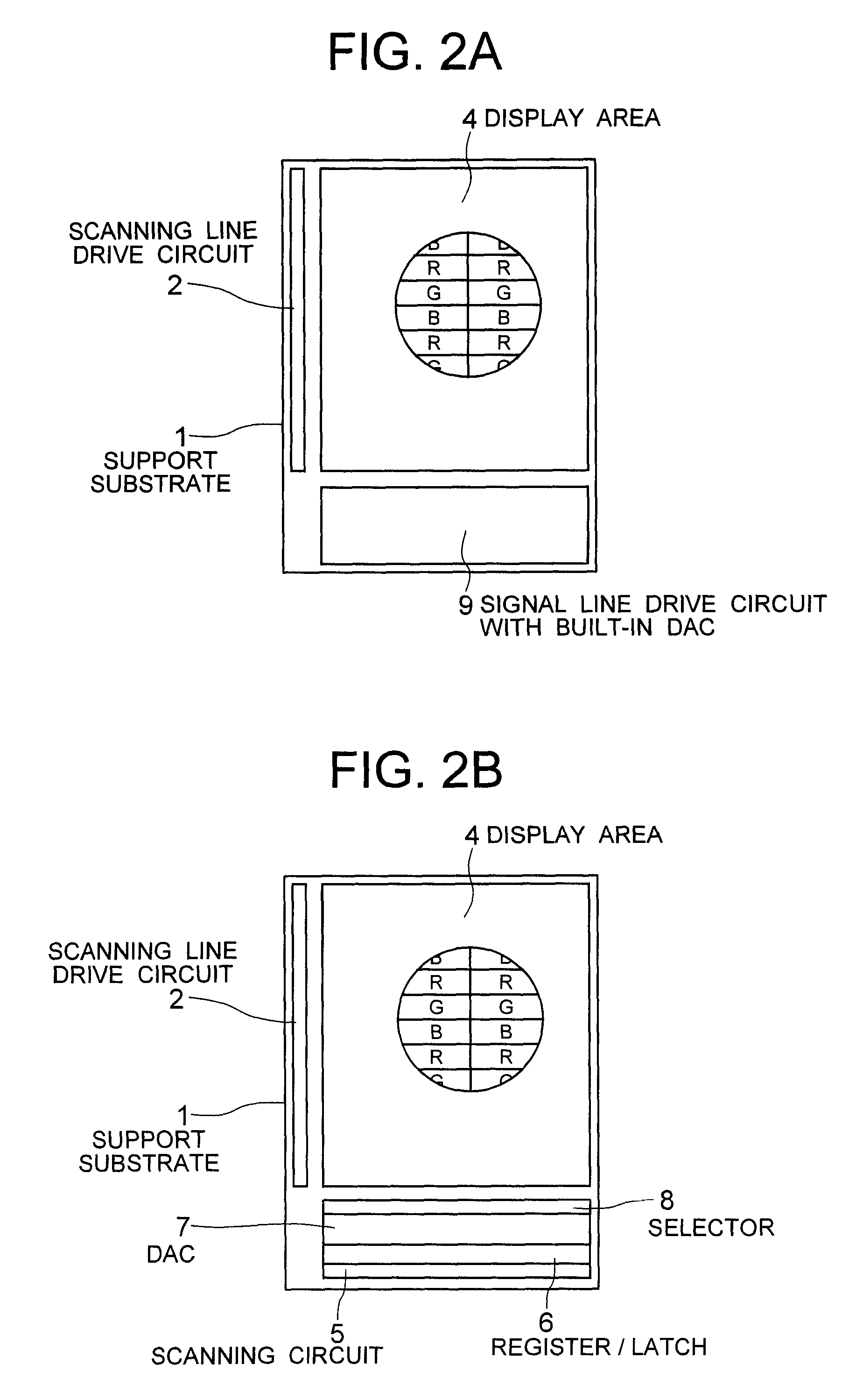
[0082]FIG. 2A is a plan view for showing the display apparatus according to the present invention. FIG. 2B is a plan view for showing an example of the signal line drive circuit in FIG. 2A. There will be explanations provided hereinafter by referring to those drawings.

first embodiment

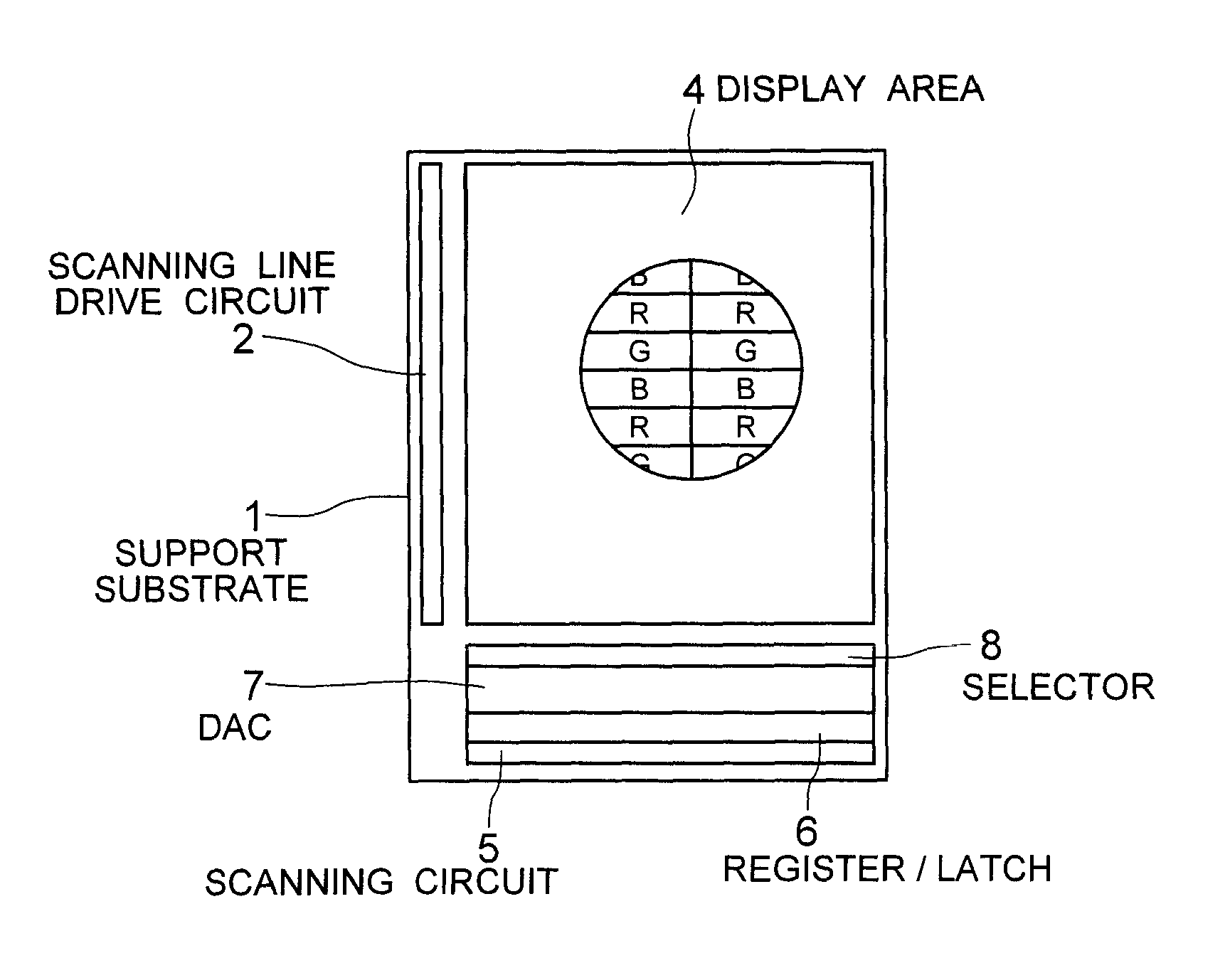
[0083]In this embodiment, more complicated circuits such as a DAC circuit and the like shown in FIG. 38 of Patent Literature 1 (FIG. 18 of this Application) are integrated, in addition to the structure of the That is, in this embodiment, a display area 4 in which pixels are provided in matrix, a scanning line drive circuit 2 for driving scanning lines, and a signal line drive circuit 9 with a built-in DAC are provided on a support substrate 1. The pixel within the display area 4 is constituted with a plurality of dots. Each dot corresponds to a color filter of a certain color. The dot is in a laterally long shape, i.e. in a shape extending in a direction along the scanning lines. In other words, each dot is in a shape extending in parallel with the longitudinal direction of the signal line drive circuit 9. The color filters are of lateral stripe type, for example.

[0084]More specifically, the signal line drive circuit 9 with a built-in DAC comprises a scanning circuit 5, a register / ...

third embodiment

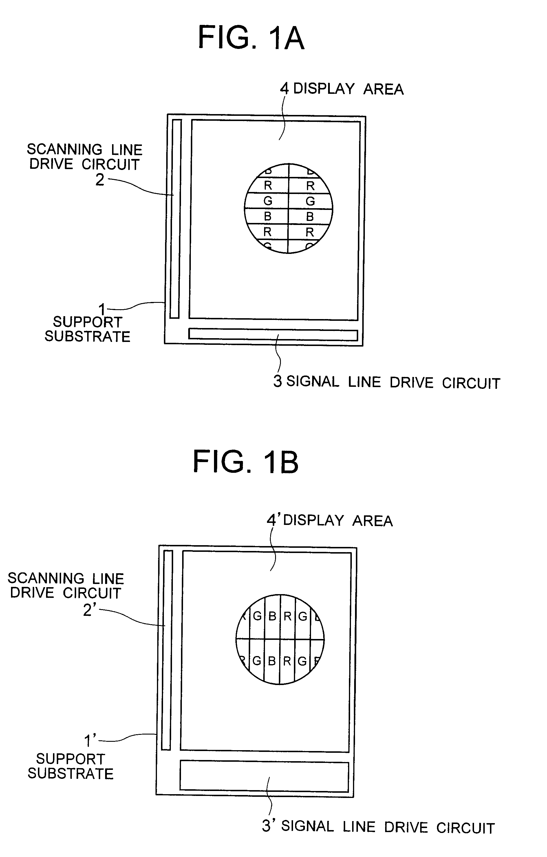
[0088]FIG. 3 is a plan view for showing the display apparatus according to the present invention. There will be explanations provided hereinafter by referring to the drawing.

[0089]This embodiment employs a structure that decreases the power consumed in an interface part through processing data in parallel by extending the bus width of data from an external IC. This structure is disclosed in Patent Literature 1. That is, in this embodiment, a display area 4 in which pixels are provided in matrix, a scanning line drive circuit 2 for driving scanning lines, and a signal line drive circuit (described later) which performs data processing in parallel by extending the bus width between outside are provided on a support substrate 1. The pixel within the display area 4 is constituted with a plurality of dots. Each dot corresponds to a color filter of a certain color. The dot is in a laterally long shape, i.e. in a shape extending in a direction along the scanning lines. In other words, each...


PUM


Abstract

Provided is a display apparatus capable of reducing the scale of a drive circuit and decreasing the frame. A display area in which pixels are provided in matrix, a scanning line drive circuit for driving scanning lines, and a signal line drive circuit for driving signal lines are provided on a support substrate. The pixel within the display area is constituted with a plurality of dots. Each dot corresponds to a color filter of a certain color. The dot is in a laterally long shape, i.e. in a shape extending in a direction along the scanning lines. In other words, each dot is in a shape extending in parallel with the longitudinal direction of the signal line drive circuit. The color filters are of lateral stripe type, for example.

Description

BACKGROUND OF THE INVENTION[0001]1. Field of the Invention[0002]The present invention relates to a display apparatus that is constituted with pixels arranged in matrix on a substrate and, in particular, to a display apparatus with built-in electronic circuits.[0003]2. Description of the Related Art[0004]Color display apparatuses such as color liquid crystal display apparatuses are used widely. Among the color display apparatuses, especially those of color-filter type using micro-color filters are broadly used mainly for the liquid crystal display apparatuses. An example of the conventional color display apparatus of the color-filter type will be described by referring to the accompanying drawings.[0005]FIG. 16 is a plan view for showing each dot (display unit of a certain color) and layout of color filters within a display area according to the example of the conventional display apparatus. Explanations thereof will be provided hereinafter by referring to this drawing.[0006]In this ...

Claims


Application Information

Patent Timeline
Patent Type & Authority Patents(United States)
IPC IPC(8): G06F3/038
CPCG09G3/20G09G3/3685G09G2300/0408G09G2300/0452G09G2310/027
Inventor TAKATORI, KENICHIASADA, HIDEKIHAGA, HIROSHI
Owner HANNSTAR DISPLAY CORPORATION
Why Eureka
Try Eureka