

Semiconductor Wafer and Method of Manufacturing the Same and Method of Manufacturing Semiconductor Device
a semiconductor and semiconductor technology, applied in the direction of semiconductor devices, semiconductor/solid-state device details, electrical equipment, etc., can solve the problems of large drag on practical application, increase in manufacturing costs of the above process, and difficulty in uniform development, etc., to achieve short tat and low cost
- Summary
- Abstract
- Description
- Claims
- Application Information
AI Technical Summary
Benefits of technology
Problems solved by technology
Method used
Image

Examples
first embodiment
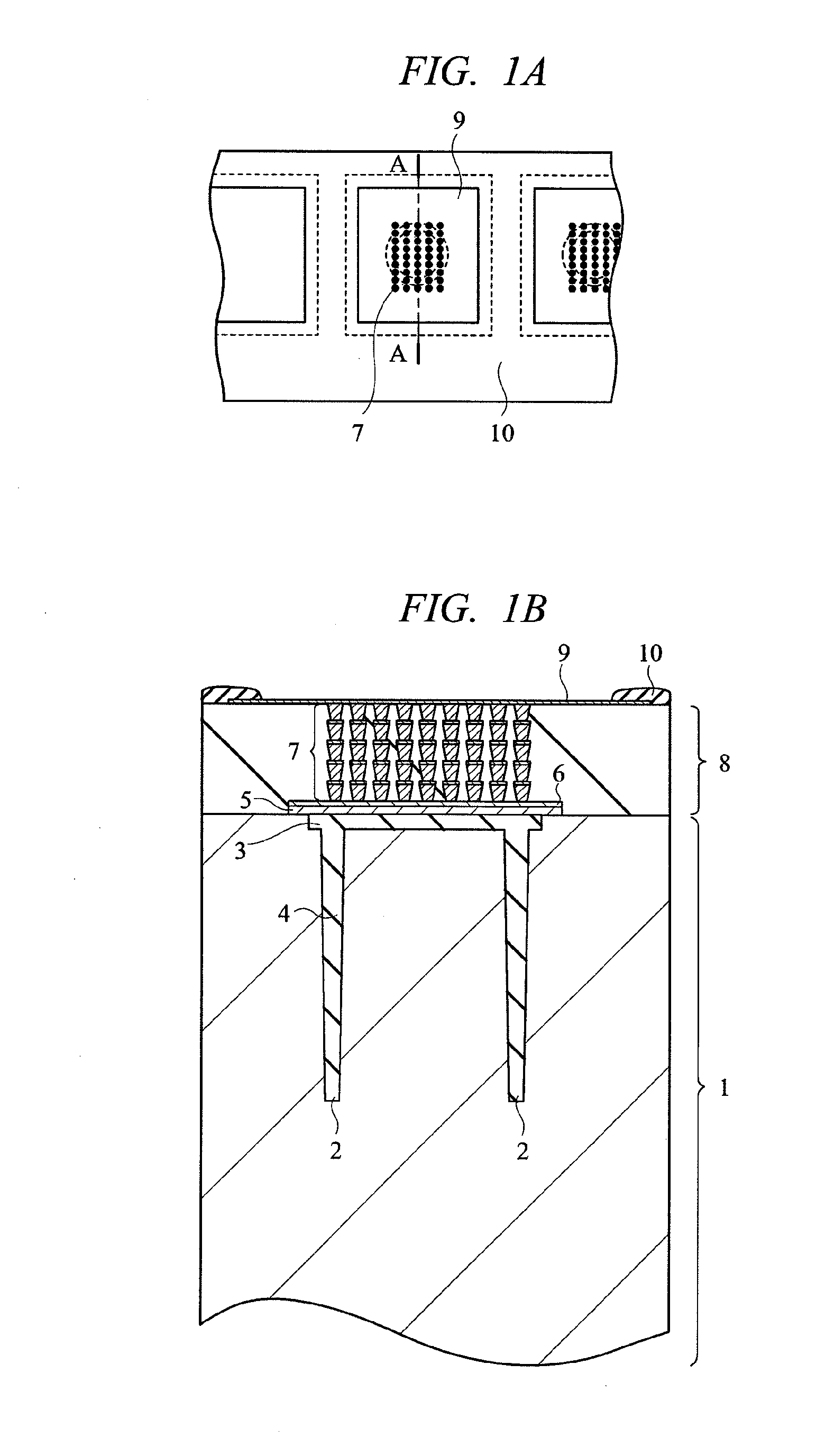
[0065]FIG. 1 includes FIG. 1A of a plan view showing main parts of a semiconductor wafer according to a first embodiment of the present invention and FIG. 1B of a cross sectional view of FIG. 1A cut along the cutting-plane line A-A.
[0066]The semiconductor wafer of the present embodiment is also capable of being distributed as a product even in a form of semiconductor wafer other than manufacturing a semiconductor device as a product using the semiconductor wafer.
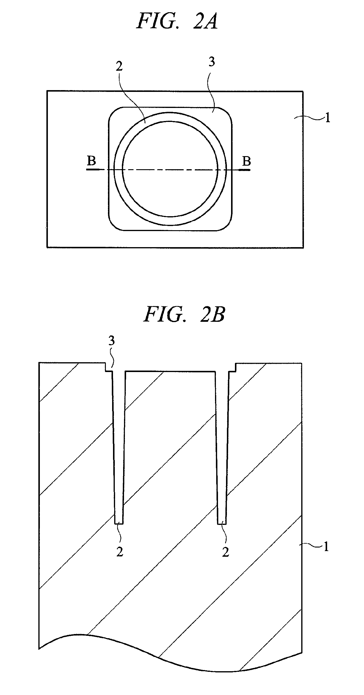
[0067]The semiconductor wafer of the present invention has, as shown in FIG. 1, a tubular deep trench 2 formed in a silicon (Si) substrate 1, and an insulating material 4 such as an oxide film which is an insulating member is filled inside and on an upper surface (field part 3) of the deep trench 2. The deep trench 2 is formed by dry etching, and the insulating material 4 is filled inside the tubular trench and the field part 3 by, for example, CVD. As an upper layer of the insulating material 4, a gate electrode film 5 such...
second embodiment
[0083]FIG. 18A and FIG. 19A are plan views showing main parts of a semiconductor wafer of a second embodiment of the invention and FIG. 18B and FIG. 19B are cross-sectional views of FIG. 18A and FIG. 19A cut along the cutting-plane line A-A.
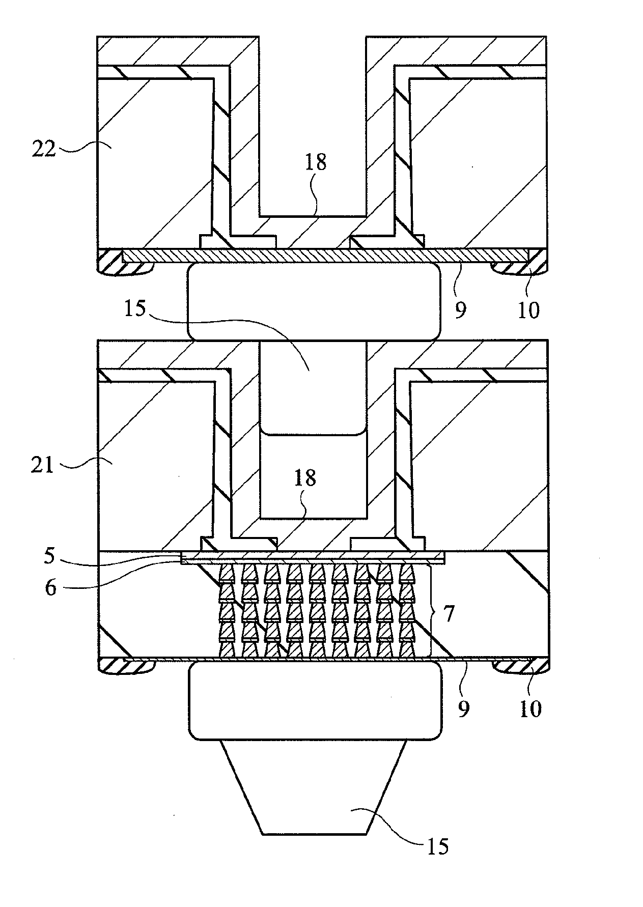
[0084]The semiconductor wafer of the present embodiment has a structure where I / O cell wirings 16 are arranged just under the external connection electrode (Al electrode and the like) 9 as shown in FIG. 18. Upon accelerating shrinkage of chip size, it is effective to put in the I / O cell wirings 16 also under an electrode pad. In the cross-sectional structure of FIG. 1, the I / O cell wiring structure is not provided under the electrode pad and it is structured only by the columnar wiring vias 7 electrically connecting between the metal film 6 and the external connection electrode 9 formed on an upper surface of the deep trench 2. In contrast, under the electrode pad, in addition to the columnar wiring vias 7 electrically connecting the metal film 6...
third embodiment
[0087]FIG. 20 to FIG. 26 are plan views and cross-sectional views showing respective manufacturing steps of a semiconductor deice using a semiconductor wafer of a third embodiment of the present invention.
[0088]In the present embodiment, a method of manufacturing an interposer chip by forming a through-hole electrode similarly to the above first embodiment on, for example, a wafer for interposer having the external connection electrodes 9 of one-layer wiring on the front / back sides is described. As shown in FIG. 20, the series of processes of: back grinding of silicon wafer (FIG. 21); dropping the silicon piece (FIG. 22); forming the insulating film 11 (FIG. 23); forming the seed layer and the electrolytic plating layer 14 (FIG. 24); and forming the stud bump 15 (FIG. 25, FIG. 26) with respect to the silicon wafer with the deep trench 2 and the external connection electrode 9 formed thereon is same as that of the product LSI described in the first embodiment. However, as shown in FI...
PUM
 Abstract
Description
Claims
Application Information