Laser processing apparatus

Inactive Publication Date: 2010-07-01
HITACHI HIGH-TECH CORP
View PDF5 Cites 5 Cited by
  • Summary
  • Abstract
  • Description
  • Claims
  • Application Information

AI Technical Summary

Benefits of technology

[0008]Accordingly, the present invention provides a laser processing appa

Problems solved by technology

However, the use of laser light for dividing the film into cells may cause such problems as low fabrication yields and failures to achieve specific characteristics.
If the laser processing accuracy is low, insulation between cells may be inadequate, resulting in a failure to attain a spec

Method used


Image

  • Laser processing apparatus
  • Laser processing apparatus
  • Laser processing apparatus

Examples


first embodiment

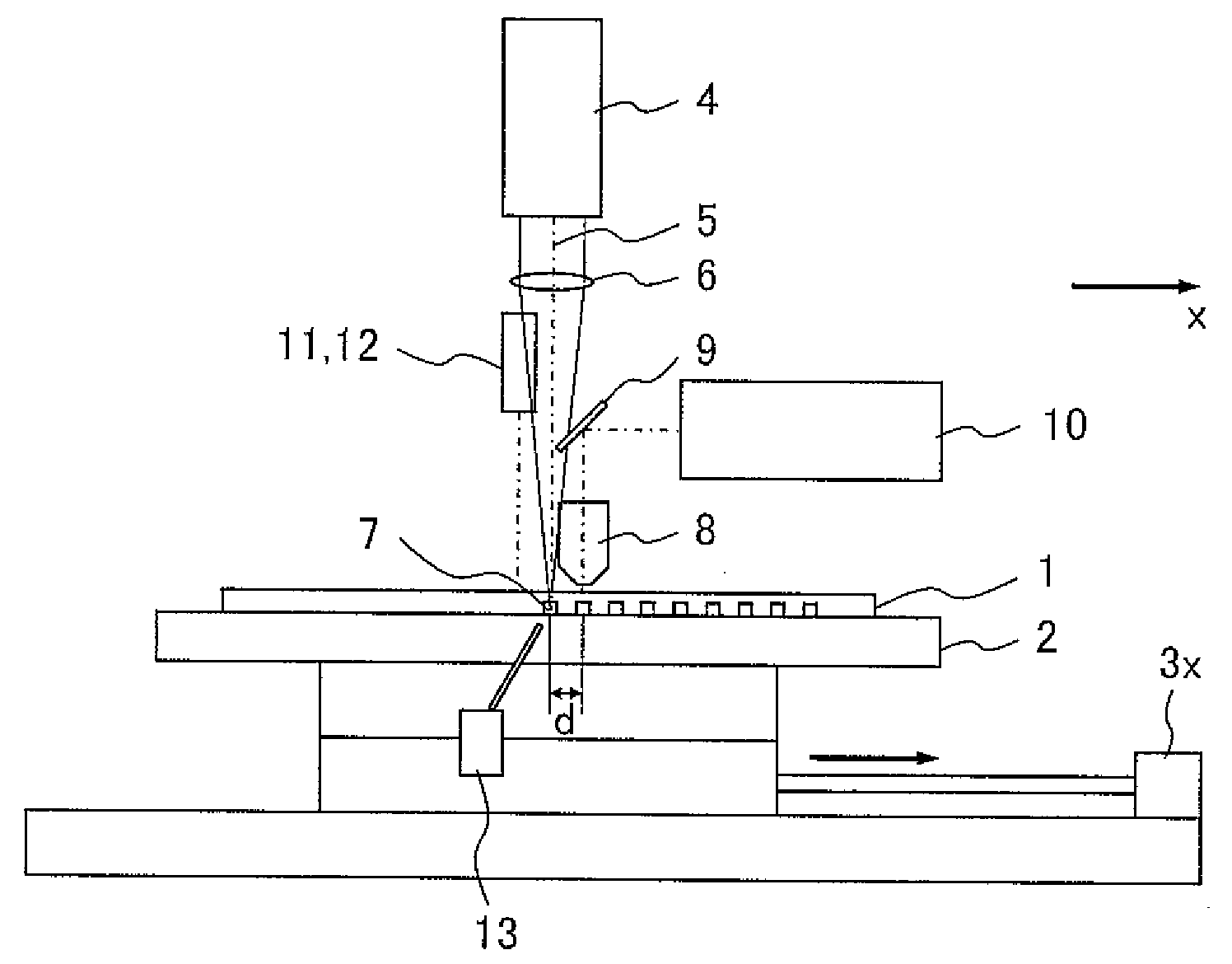
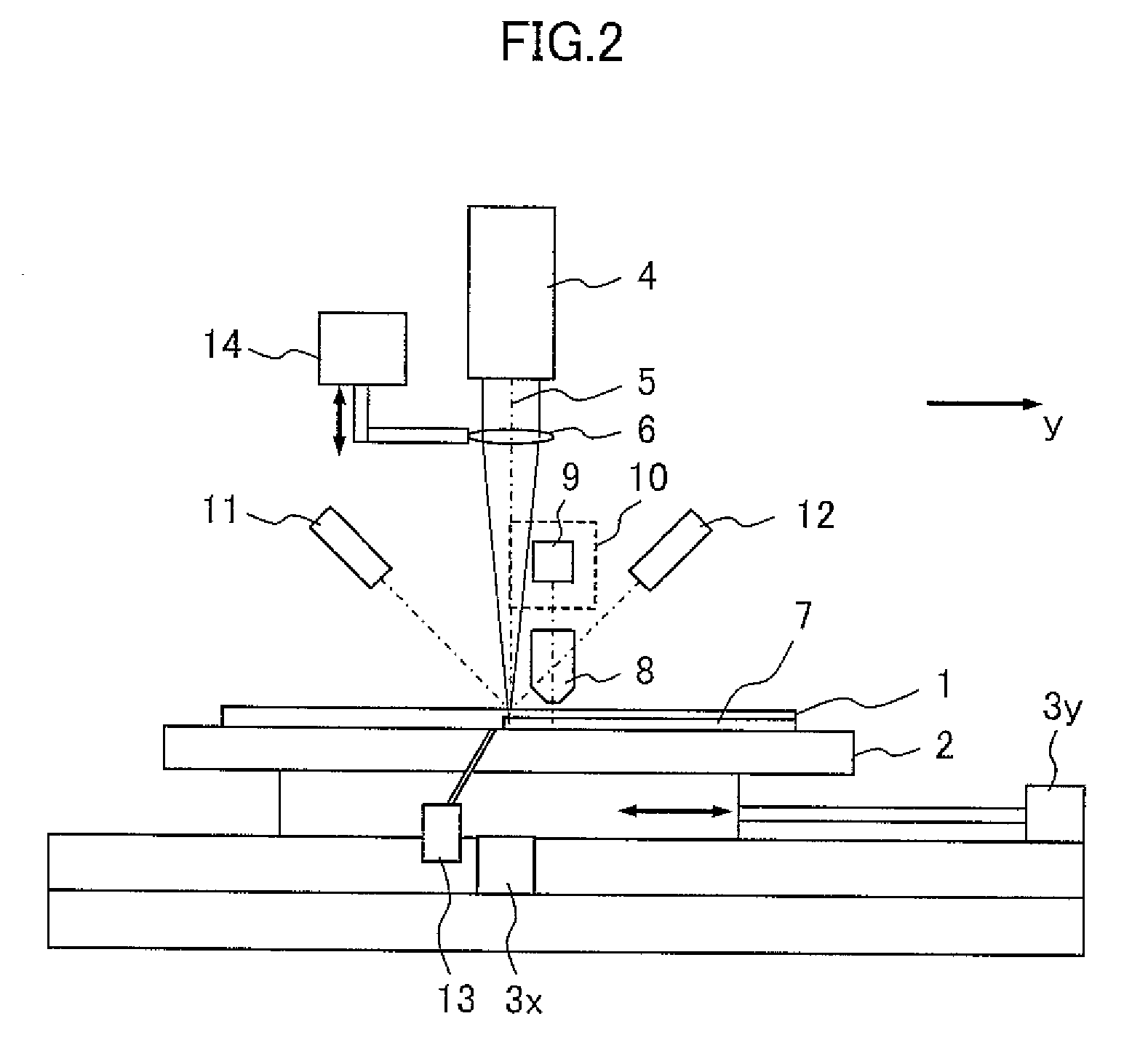
[0029]A first embodiment of the invention is described below referring to FIGS. 1 to 3, FIGS. 4A to 4G and FIGS. 5A to 5C.

[0030]FIGS. 1, 2 and 3 show the apparatus according to the first embodiment as viewed from the y direction, x direction and z direction, respectively. Reference numeral 1 denotes a substrate, 2 a stage, 3x an x-axis moving mechanism, 3y a y-axis moving mechanism, 4 a laser optics system, 5 laser light, 6 a condenser lens, 7 laser-processed grooves, 8 an objective lens, 9 a mirror, 10 an observation device, 11 a displacement gauge light source, 12 a photo-detector for the displacement gauge, 13 a mechanism for blowing off foreign matter, 14 a focusing mechanism, and 15 a base. The laser radiation section includes the laser optics system 4 and condenser lens 6. The optical inspection section includes the objective lens 8, mirror 9, and observation device 10. The undulation measurement section includes the displacement gauge light source 11 and displacement gauge ph...

second embodiment

[0057]Next, an example of optical inspection as a second embodiment of the invention will be explained referring to FIG. 6 and FIGS. 7A and 7B. Regarding things that have been described concerning the first embodiment and are not described below, they also hold true for the second embodiment.

[0058]FIG. 6 shows details of an optical inspection section according to the second embodiment; and FIG. 7A shows the shape of a laser-processed groove and FIG. 7B shows output data from a detector 25 of the optical inspection section. In FIG. 6, reference numeral 1 denotes a substrate and 7 denotes a processed groove. The optical inspection section includes an objective lens 8 and mirror 9 as in the first section and also includes, as components of an observation device, a laser light source for observation 21, translucent mirror 22, lens 23, aperture 24, and detector 25. When the focal point of the lens 23 is aligned with the aperture 24, the device functions as a confocal laser scanning micro...

third embodiment

[0061]Next, another example of optical inspection as a third embodiment will be explained referring to FIG. 8 and FIGS. 9A and 9B. Regarding things that have been described concerning the first embodiment and are not described below, they also hold true for the third embodiment.

[0062]FIG. 8 shows details of an optical inspection section according to the third embodiment. In FIG. 8, reference numeral 1 denotes a substrate and 7 denotes a processed groove. The optical inspection section includes a dark-field objective lens 31, mirror with a hole 32, lenses 34a and 34b, light source 33 and detector 35.

[0063]This embodiment uses a dark-field microscope as an observation device. Through this microscope, a surface roughness of the processed groove or leavings on it which would be invisible through an ordinary microscope can be detected. Therefore, inadequate cuts in laser-processed grooves or adhesion of foreign matter can be easily located.

[0064]The light quantity distribution in the y d...


PUM

PropertyMeasurementUnit
Thicknessaaaaaaaaaa
Electrical resistanceaaaaaaaaaa
Electrical conductoraaaaaaaaaa

Abstract

A laser processing apparatus which achieves both shorter TAT and reduction in processing defects. In the apparatus, a laser radiation section, an undulation measurement section for measuring undulation of a substrate or a film thickness measuring section for measuring the thickness of a thin film formed on the substrate, and an optical inspection section for optically inspecting grooves formed by laser-processing the thin film on the substrate are fixed so that their positional relationship is kept constant.

Description

FIELD OF THE INVENTION[0001]The present invention relates to laser processing apparatuses for processing thin film.BACKGROUND OF THE INVENTION[0002]For the manufacture of thin-film solar cells having amorphous silicon thin film, microcrystal silicon thin film and / or transparent electrodes, Japanese Patent Application[0003]Laid-Open Publication No. 2005-235920 discloses a technique that laser beams are used to process such thin film. Also, Japanese Patent Application Laid-Open Publication No. 8 (1996)-37317 describes a defect detection method for thin-film solar cells and Japanese Patent Application Laid-Open Publication No. 2 (1990)-281133 describes a system which locates a short circuit defect between electrodes or wirings in a thin-film semiconductor device and repairs it.SUMMARY OF THE INVENTION[0004]In techniques of manufacturing thin-film solar cells which use amorphous silicon or microcrystal silicon, a sheet electricity-generating layer and transparent conductive film are sep...

Claims


Application Information

Patent Timeline
IPC IPC(8): H01L21/66H01L21/306B23K26/00B23K26/364H01L31/04H01S3/00
CPCB23K26/0853Y02E10/50H01L31/046B23K2103/172B23K26/364B23K26/40B23K26/702
Inventor YAMAGUCHI, HIRONARUHONGO, MIKIOKOIZUMI, MITSUYOSHIARAKI, MASAKI
Owner HITACHI HIGH-TECH CORP
Why Eureka
Try Eureka