Substrate processing apparatus and substrate processing method

a substrate processing and substrate technology, applied in the direction of liquid/solution decomposition chemical coating, manufacturing tools, coatings, etc., can solve the problems of defective processing in a local or global region of the substrate, the contact efficiency between the processing liquid and the substrate can decrease, and the defective processing becomes more marked, so as to achieve high yield and reduce the cost of electronic products.

Inactive Publication Date: 2005-11-03
EBARA CORP +1
View PDF3 Cites 1 Cited by
  • Summary
  • Abstract
  • Description
  • Claims
  • Application Information

AI Technical Summary

Benefits of technology

[0021] According to the present invention, static electricity on a surface of the substrate is arbitrarily adjusted prior to carrying out wet processing of the surface of the substrate. This makes it possible to produce an LSI or the like in a high yield even in a future generation when finer interconnects of more advanced material are employed. The present invention can thus contribute to cost reduction of electronic products.

Problems solved by technology

Further, in case a liquid chemical (processing liquid), such as a plating solution, for wet processing has a polarity, the contact efficiency between the processing liquid and the substrate can decrease, which can result in defective processing in a local or global region of the substrate.
This defective processing becomes more marked as the processing size of substrate decreases.
For example, a decrease in yield due to defective processing becomes a considerable problem when forming 90 nm-node or later-generation interconnects by the above-described damascene process, though it is negligible with 130 nm-node interconnects.
Further, the type of interconnect material affects defective processing.
In addition, use of a low-k material, such as an organic material or a porous material, for an insulating film increases defective processing.

Method used


Image

  • Substrate processing apparatus and substrate processing method
  • Substrate processing apparatus and substrate processing method
  • Substrate processing apparatus and substrate processing method

Examples


Embodiment Construction

[0032] Preferred embodiments of the present invention will now be described with reference to the drawings.

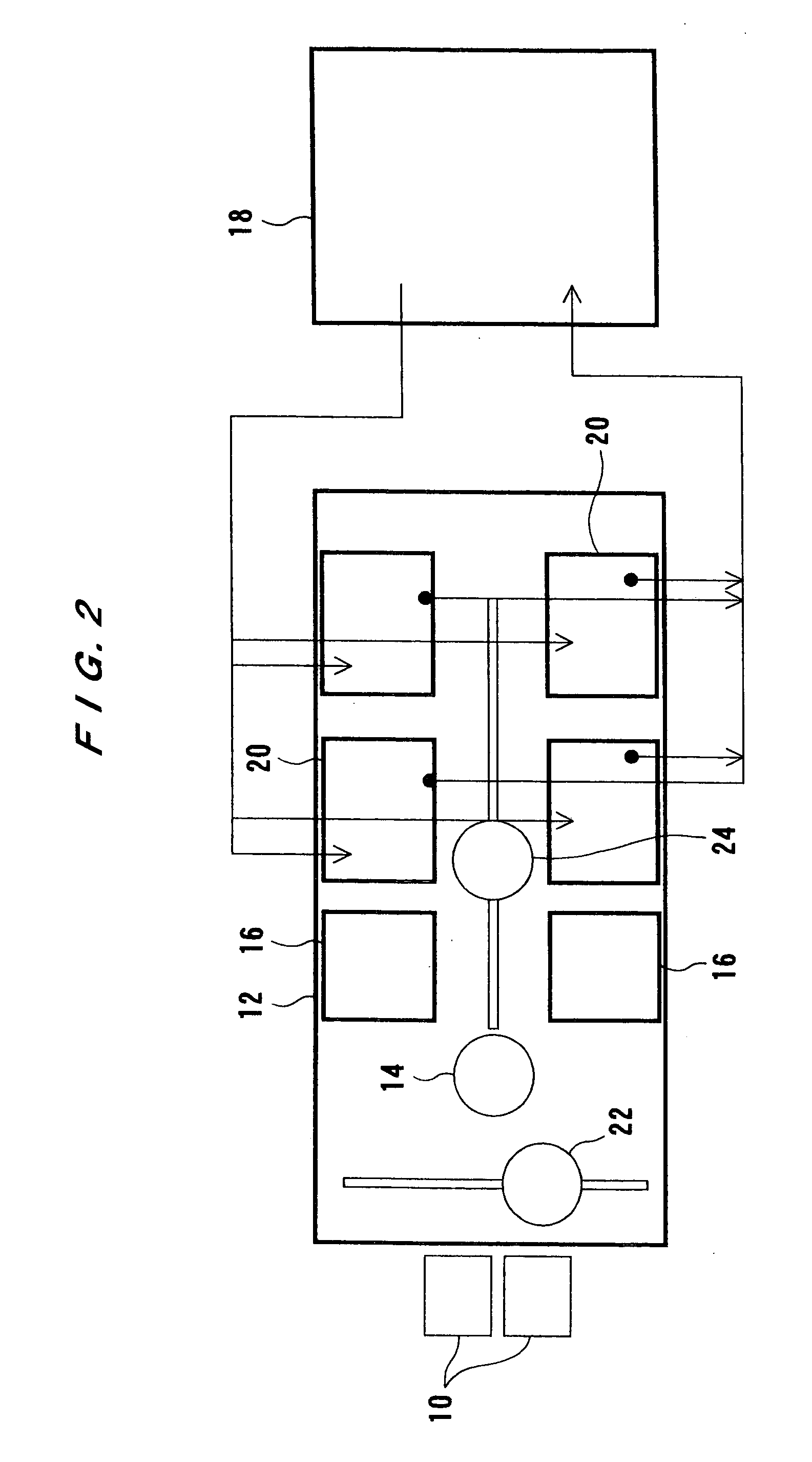
[0033]FIG. 3 shows a layout plan of a substrate processing apparatus, adapted to carry out electroplating, according to an embodiment of the present invention. The substrate processing apparatus, as with the substrate processing apparatus shown in FIG. 2, includes an apparatus frame 12. A substrate in a dry state is carried into the apparatus frame 12 from a substrate cassette 10; the substrate is processed inside the apparatus frame 12; and the substrate after processing, in a dry state, is taken out of the apparatus frame 12. Inside the apparatus frame 12 are disposed a stage 14, two post-cleaning apparatuses 16, four electroplating apparatuses 20 connected via piping to a plating solution supply / recovery apparatus 18, a first substrate transport robot 22 and a second substrate transport robot 24.

[0034] The substrate processing apparatus of this embodiment is also provided ...


PUM

PropertyMeasurementUnit
conductiveaaaaaaaaaa
polarityaaaaaaaaaa
processing sizeaaaaaaaaaa

Abstract

A substrate processing apparatus and a substrate processing method can appropriately control the charge of a substrate depending on the type of wet processing, thereby reducing defective processing due to static electricity on the surface of the substrate. The substrate processing apparatus includes: a static electricity adjustment section for adjusting static electricity on a substrate; and a wet processing apparatus for carrying out wet processing of the static electricity-adjusted substrate. The static electricity adjustment section removes static electricity from the substrate or charges the substrate into a desired charged state, for example.

Description

BACKGROUND OF THE INVENTION [0001] 1. Field of the Invention [0002] The present invention relates to a substrate processing apparatus and a substrate processing method, and more particularly to a substrate processing apparatus and a substrate processing method which are useful for carrying out wet processing of a surface of the substrate by bringing the surface of the substrate into contact with a processing liquid, such as a liquid chemical or pure water. [0003] 2. Description of the Related Art [0004] In place of dry processes which have been principally employed for the formation of LSI interconnects or the like on a semiconductor substrate, wet processes, such as plating, chemical-mechanical polishing (CMP), electrolytic etching, electrolytic polishing and cleaning, are increasing being employed these days. For example, a so-called damascene process, which comprises embedding a metal (conductive material), such as aluminum, and more recently silver or copper, by plating into int...

Claims


Application Information

Patent Timeline
Patent Type & Authority Applications(United States)
IPC IPC(8): C23C18/16C23F1/00C23F1/08C23C18/18C23G3/02C25D5/34C25D7/12C25D17/00C25D21/12C25F3/12C25F3/30C25F7/00H01L21/00H01L21/02H01L21/304H01L21/306H01L21/3063
CPCC23C18/1632C23F1/08C23G3/027C25D5/34C25D17/00H01L21/6723C25F7/00H01L21/02063H01L21/02074H01L21/67173C25D21/12
Inventor MISHIMA, KOJISUZUKI, HIDENAONOMURA, KAZUFUMIKANEKO, HISASHITOYODA, HIROSHI
Owner EBARA CORP
Why Eureka
Try Eureka