Method for making a charge balanced multi-nano shell drift region for superjunction semiconductor device

Active Publication Date: 2011-02-22
ALPHA & OMEGA SEMICON INC
25 Cites 39 Cited by

AI-Extracted Technical Summary

Problems solved by technology

Upon depletion, the stripes appear to be an ‘intrinsic’ layer and a near uniform electric field distribution is achieved, resulting in a high breakdown voltage.
A typical diffusion process may require a temperature of 1150 degree C. for 6-10 hrs thus entailing an undesirable high thermal budget.
Another disadvantage of this method is, for charge balanced st...

Method used

[0049]In FIG. 2B, a cavity-shaped doped epitaxial layer-1171 is formed, via selective epitaxial growth (SEG) through the mask window 158a, upon the vertical cavity 162 while insuring that the doping parameters and thickness of the doped epitaxial layer-1171 correspond respectively to the desired conductivity type and shell thickness of the outermost nano shell member. In FIG. 2C, the bottom portion of the just formed doped epitaxial layer-1171 is anisotropically etched away, through the mask window 158a, hence forming a nano shell member (NSM1) 171a. From FIG. 2D through FIG. 2E the same steps illustrated in FIG. 2B and FIG. 2C are repeated to form a cavity-shaped doped epitaxial layer-2172 and then a nano shell member (NSM2) 172a. The same steps are then repeated to successively form, inside the vertical cavity 162, additional nano shell members (NSM3) 173a, NSM4174a, NSMS 175a and NSM6176a so as to successively fill the vertical cavity 162 till a residual space 177 of residual space depth RSD and residual space width RSW remains therein. The thus fabricated NSM1171a through NSM6176a form a number of contiguous, concentric nano shell members and are illustrated in FIG. 2F. Furthermore, to realize a substantially charge balanced MNSDR, the NSM1171a through NSM6176a are formed of alternating, substantially charge balanced first conductivity type and sec...

Benefits of technology

[0035]Under the second embodiment, the fill-up nano plate can be formed by forming, inside the residual space, a fill-up material whose charge balance property is insensitive to internal voids formation typically observed under a high aspect ratio ...

Abstract

A method is disclosed for making a substantially charge balanced multi-nano shell drift region (MNSDR) for superjunction semiconductor devices atop a base substrate. The MNSDR has numerous concentric nano shell members NSM1, NSM2, . . . , NSMM (M>1) of alternating, substantially charge balanced first conductivity type and second conductivity type and with height NSHT. First, a bulk drift layer (BDL) is formed atop the base substrate. A substantially vertical cavity of pre-determined shape and size and with depth NSHT is then created into the top surface of BDL. The shell members NSM1, NSM2, . . . , NSMM are successively formed inside the vertical cavity, initially upon its vertical walls then moving toward its center, so as to successively fill the vertical cavity till a residual space remains therein. A semi-insulating or insulating fill-up nano plate is then formed inside the residual space to fill it up.

Application Domain

Semiconductor/solid-state device manufacturingSemiconductor devices

Technology Topic

Semi insulatingEngineering +5

Image

  • Method for making a charge balanced multi-nano shell drift region for superjunction semiconductor device
  • Method for making a charge balanced multi-nano shell drift region for superjunction semiconductor device
  • Method for making a charge balanced multi-nano shell drift region for superjunction semiconductor device

Examples

  • Experimental program(2)

Example

[0048]FIG. 2A through FIG. 2G illustrate a first embodiment method of making the MNSDR under the present invention. In FIG. 2A a BDL 156 is formed. In one embodiment, the BDL 156 may be formed atop a base substrate (not shown here to avoid unnecessary obscuring details). In another alternative embodiment, a buffer layer may be formed between the BDL and the base substrate. As an example, the BDL 156 can be formed by epitaxially growing the BDL 156 with doping parameters known in the art and corresponding to a desired conductivity type and dopant concentration. As a more specific example, the BDL 156 can be formed with a very low N− dopant volumetric concentration in the range of from about 1E14-cm-3 to about 1E16-cm-3. A cavity hard mask 158 is then applied atop the BDL 156 and opened with a mask window 158a of pre-determined shape and size CVS. The BDL 156 is then anisotropically etched through the mask window 158a to create a substantially vertical cavity 162 with a depth NSHT. As an application example, CVS can range from about 5 microns to about 40 microns while NSHT can range from about 5 microns to about 50 microns. It should be pointed out that, in practice, the “substantially vertical” walls of the vertical cavity 162 may have a taper of around five (5) degrees from the vertical.
[0049]In FIG. 2B, a cavity-shaped doped epitaxial layer-1171 is formed, via selective epitaxial growth (SEG) through the mask window 158a, upon the vertical cavity 162 while insuring that the doping parameters and thickness of the doped epitaxial layer-1171 correspond respectively to the desired conductivity type and shell thickness of the outermost nano shell member. In FIG. 2C, the bottom portion of the just formed doped epitaxial layer-1171 is anisotropically etched away, through the mask window 158a, hence forming a nano shell member (NSM1) 171a. From FIG. 2D through FIG. 2E the same steps illustrated in FIG. 2B and FIG. 2C are repeated to form a cavity-shaped doped epitaxial layer-2172 and then a nano shell member (NSM2) 172a. The same steps are then repeated to successively form, inside the vertical cavity 162, additional nano shell members (NSM3) 173a, NSM4174a, NSMS 175a and NSM6176a so as to successively fill the vertical cavity 162 till a residual space 177 of residual space depth RSD and residual space width RSW remains therein. The thus fabricated NSM1171a through NSM6176a form a number of contiguous, concentric nano shell members and are illustrated in FIG. 2F. Furthermore, to realize a substantially charge balanced MNSDR, the NSM1171a through NSM6176a are formed of alternating, substantially charge balanced first conductivity type and second conductivity type semiconductor materials. NSM1171a through NSM6176a are formed with appropriate conductivity type, doping concentration and width to achieve substantial charge balance.
[0050]In FIG. 2G, the residual space 177 is filled up with the formation of a semi-insulating or insulating fill-up nano plate 178 therein, for example a fill-up oxide nano plate 178 as illustrated. Alternatively the fill-up nano plate could be intrinsic silicon/semiconductor material. Notice the high aspect ratio RSD/RSW of the fill-up oxide nano plate 178. While internal voids formation are typically observed inside the fill-up oxide nano plate 178 with such a high aspect ratio, the usage of semi-insulating or insulating fill-up materials therein makes the resulting charge balance property of the MNSDR insensitive to such internal voids. As a more specific embodiment, the host semiconductor material for both base substrate and the BDL 156 is silicon and the fill-up material is silicon oxide or intrinsic silicon. Afterwards, the windowed cavity mask 158 is removed from the top of the MNSDR (not shown).

Example

[0051]FIG. 3A through FIG. 3G illustrate a second embodiment method of making the MNSDR under the present invention similar to the method illustrated in FIG. 2A through FIG. 2G. However in FIG. 3A through FIG. 3G, a hard mask is not used during the growing of the NSM's. In FIG. 3A a BDL 156 is formed atop a base substrate (not shown here to avoid unnecessary obscuring details). The BDL 156 can be formed by epitaxially growing the BDL 156 with doping parameters known in the art and corresponding to a desired conductivity type and dopant concentration. A cavity mask 158 is then applied atop the BDL 156 and opened with a mask window 158a of pre-determined shape and size CVS. The BDL 156 is then anisotropically etched through the mask window 158a to create a substantially vertical cavity 162 with a depth NSHT. As pointed out before, in practice, the “substantially vertical” walls of the vertical cavity 162 has a taper of around five (5) degrees from the vertical. The windowed cavity mask 158 is then completely removed, as shown in FIG. 3A.
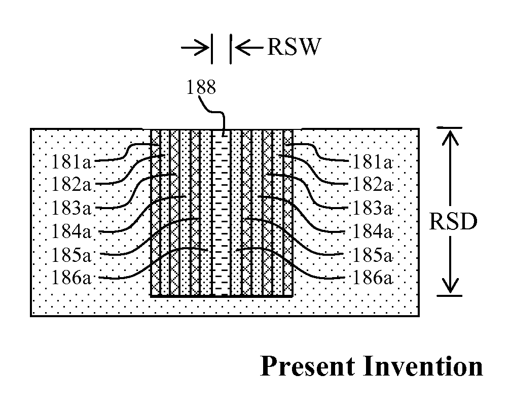
[0052]In FIG. 3B, a doped epitaxial layer-1181 with a cavity-shaped central portion is formed via epitaxial growth (EPG) atop while insuring that the doping parameters and thickness of the doped epitaxial layer-1181 correspond respectively to the desired conductivity type and shell thickness of the outermost nano shell member. The doped epitaxial layer-1181 is non-selectively grown on all exposed semiconductor surfaces. In FIG. 3C, the horizontal surface portions of the just formed doped epitaxial layer-1181 are anisotropically etched away thus forming a nano shell member (NSM1) 181a. From FIG. 3D through FIG. 3E the same steps illustrated in FIG. 3B and FIG. 3C are repeated to form a doped epitaxial layer-2182 and then a nano shell member (NSM2) 182a. The same steps are then repeated to successively form, inside the vertical cavity 162, additional nano shell members NSM3 183a, NSM4 184a, NSM5 185a and NSM6 186a so as to successively fill the vertical cavity 162 till a residual space 187 of residual space depth RSD and residual space width RSW remains therein. The thus fabricated NSM1181a through NSM6186a form a number of contiguous, concentric nano shell members and are illustrated in FIG. 3F. Furthermore, to realize a substantially charge balanced MNSDR, the NSM1181a through NSM6186a are formed of alternating, substantially charge balanced first conductivity type and second conductivity type semiconductor materials.
[0053]In FIG. 3G, the residual space 187 is filled up with the formation of a semi-insulating or insulating fill-up nano plate therein, for example a fill-up oxide nano plate 188 as illustrated. Notice the high aspect ratio RSD/RSW of the fill-up oxide nano plate 188. While internal voids formation are typically observed inside the fill-up oxide nano plate 188 with such a high aspect ratio, the usage of semi-insulating or insulating fill-up materials therein makes the resulting charge balance property of the MNSDR insensitive to such internal voids. The NSM members may continue as rows in the Y-direction, or formed closed structures like those shown in FIG. 1B and FIG. 1C.
[0054]A method has been invented for making a substantially charge balanced MNSDR for superjunction semiconductor device atop a base substrate. Referring to FIG. 2F and FIG. 3F, as the various charge balanced vertical stripes within the vertical cavity 162 are fabricated in pairs the corresponding process throughput is accordingly increased. Additionally, the present invention method does not require an undesirable high temperature, long diffusion process entailing high thermal budget. Furthermore, the charge balance property of the resulting MNSDR is not disturbed by internal voids formation typically observed inside the fill-up nano plate that would otherwise affect the fabrication process yield. While the present invention has been described with examples of vertical cavity shape like rectangle and hexagon, by now it should become clear to those skilled in the art that the present invention method expects to be applicable to a wide variety of other shapes such as square, rhombus, polygon, rows, ellipse or circle, etc. The NSM's may also be formed with varying widths, and doping concentrations, so long as they are made to charge balance with their adjacent regions.
[0055]Throughout the description and drawings, numerous exemplary embodiments were given with reference to specific configurations. It will be appreciated by those of ordinary skill in the art that the present invention can be embodied in numerous other specific forms and those of ordinary skill in the art would be able to practice such other embodiments without undue experimentation. The scope of the present invention, for the purpose of the present patent document, is hence not limited merely to the specific exemplary embodiments of the foregoing description, but rather is indicated by the following claims. Any and all modifications that come within the meaning and range of equivalents within the claims are intended to be considered as being embraced within the spirit and scope of the present invention.

PUM

no PUM

Description & Claims & Application Information

We can also present the details of the Description, Claims and Application information to help users get a comprehensive understanding of the technical details of the patent, such as background art, summary of invention, brief description of drawings, description of embodiments, and other original content. On the other hand, users can also determine the specific scope of protection of the technology through the list of claims; as well as understand the changes in the life cycle of the technology with the presentation of the patent timeline. Login to view more.
Why Eureka
Try Eureka