Lateral bipolar junction transistor with reduced base resistance

a base resistance technology, applied in the field of cmos-based lateral bipolar junction transistors, can solve the problems of reducing the performance of cmos-based bipolar devices fabricated with progressively reduced dimensions, and achieve the effect of reducing the base resistan

Active Publication Date: 2011-03-01
MEDIATEK INC
View PDF3 Cites 13 Cited by
  • Summary
  • Abstract
  • Description
  • Claims
  • Application Information

AI Technical Summary

Benefits of technology

[0007]It is one object of this invention to provide a CMOS-based lateral bipolar junction transistor (lateral BJT) with reduced base resistance.

Problems solved by technology

However, there is considerable challenge in optimizing the performance of both CMOS and bipolar devices fabricated with progressively reduced dimensions.

Method used


Image

  • Lateral bipolar junction transistor with reduced base resistance
  • Lateral bipolar junction transistor with reduced base resistance
  • Lateral bipolar junction transistor with reduced base resistance

Examples


Embodiment Construction

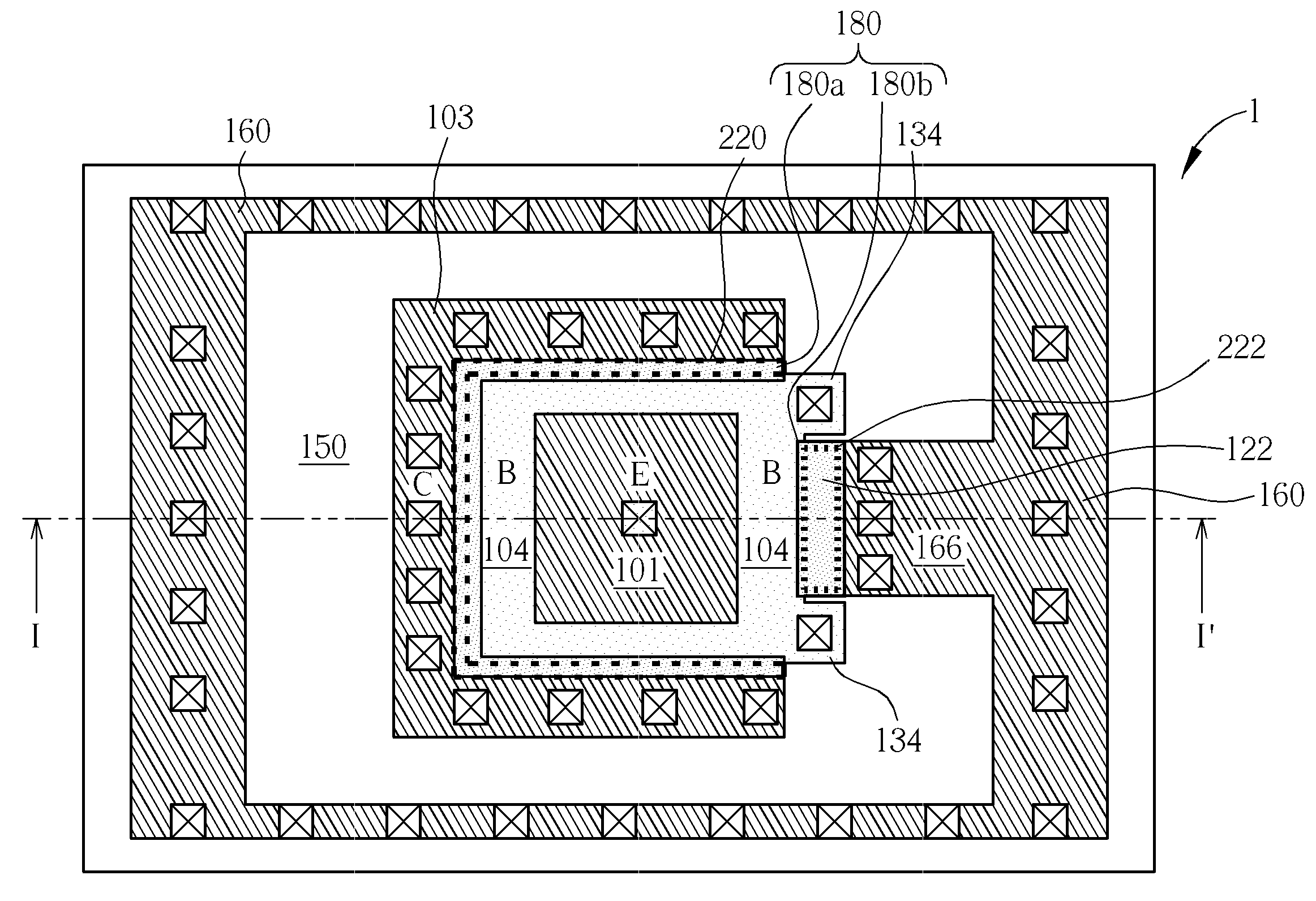
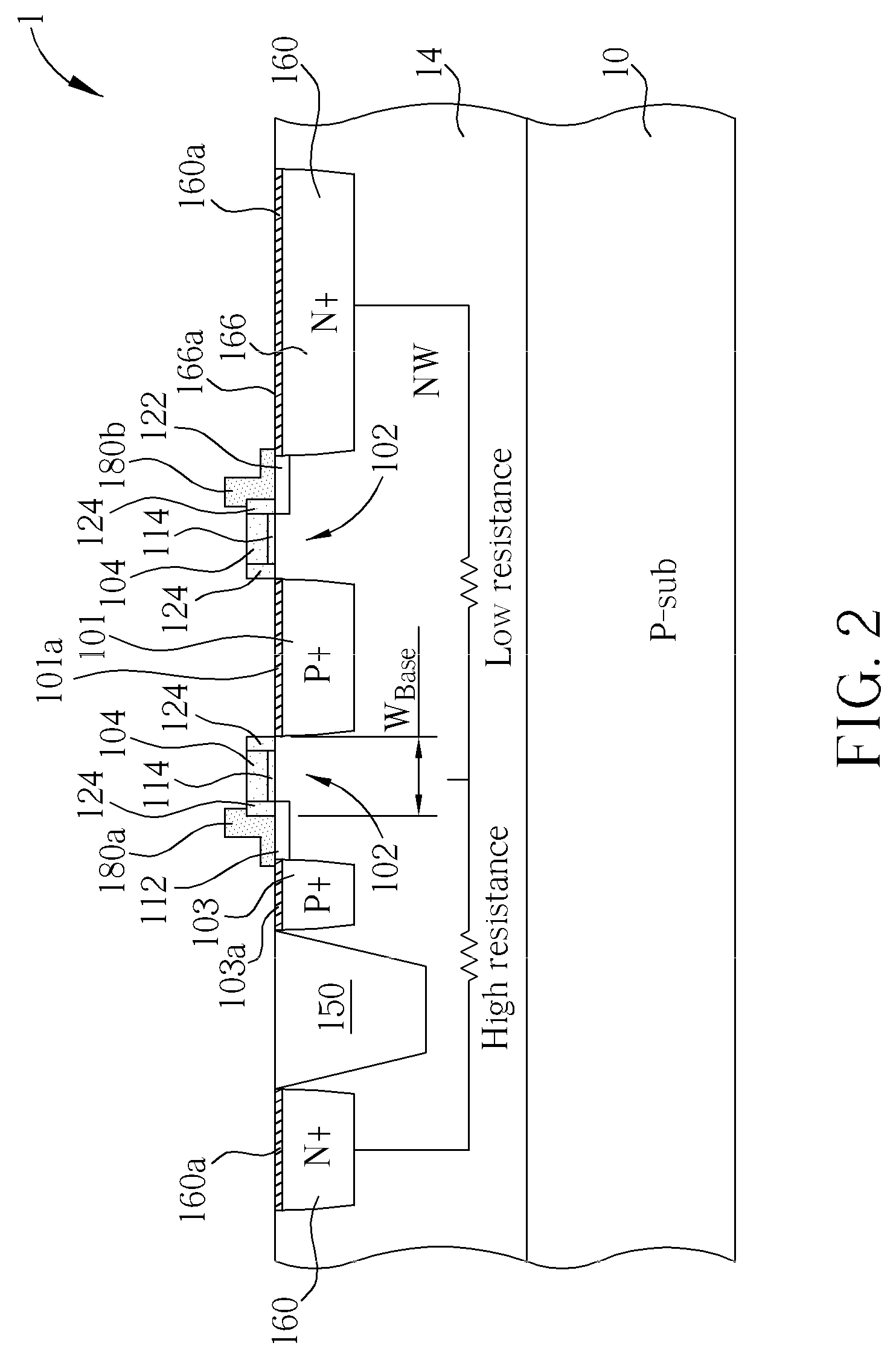
[0013]The structure and layout of the present invention lateral bipolar junction transistor (LBJT) with reduced base resistance are described in detail. The improved LBJT structure is described for a lateral PNP bipolar transistor, but it should be understood by those skilled in the art that by reversing the polarity of the conductive dopants lateral NPN bipolar transistors can be made.

[0014]Please refer to FIG. 1 and FIG. 2. FIG. 1 is a top planar view of a layout of the lateral bipolar transistor according to one embodiment of the invention. FIG. 2 is a schematic, cross-sectional view of the transistor in FIG. 1, taken along line I-I′ of FIG. 1. As shown in FIG. 1 and FIG. 2, the lateral PNP bipolar transistor 1 is formed in a semiconductor substrate 10 such as a P type doped silicon substrate. The lateral PNP bipolar transistor 1 may include a P+ doped region 101 that functions as an emitter region of the lateral PNP bipolar transistor 1, which may be formed within an N well (NW)...


PUM


Abstract

A lateral bipolar junction transistor formed in a semiconductor substrate includes an emitter region; a base region surrounding the emitter region; a gate disposed at least over a portion of the base region; a collector region having at least one open side and being disposed about a periphery of the base region; a shallow trench isolation (STI) region disposed about a periphery of the collector region; a base contact region disposed about a periphery of the STI region; and an extension region merging with the base contact region and laterally extending to the gate on the open side of the collector region.

Description

BACKGROUND OF THE INVENTION[0001]1. Field of the Invention[0002]The invention relates to the field of semiconductor technology and, more particularly, to a CMOS-based lateral bipolar junction transistor (lateral BJT) with reduced base resistance.[0003]2. Description of the Prior Art[0004]Bipolar junction transistors or bipolar transistors, which are formed using a CMOS compatible process, are well known in the art. These bipolar transistors are also referred to as lateral bipolar junction transistors and have high threshold frequency (Ft) and high beta.[0005]In the design of semiconductor integrated circuits, it is often desirable to provide a mixed mode device, i.e., which has both BJT and CMOS functions. Mixed mode devices both increase the flexibility of the IC design and increase the performance of the IC. The integration of CMOS transistors with bipolar transistors to provide Bipolar-CMOS (BiCMOS) integrated circuits is now well established. BiCMOS circuits provide advantages s...

Claims


Application Information

Patent Timeline
Patent Type & Authority Patents(United States)
IPC IPC(8): H01L29/735
CPCH01L29/0692H01L29/423H01L29/735
Inventor YANG, MING-TZONGCHENG, TAOKO, CHING-CHUNGLEE, TUNG-HSING
Owner MEDIATEK INC
Why Eureka
Try Eureka