
Method of producing SIMOX wafer

a technology of soi and simox, which is applied in the direction of semiconductor/solid-state device manufacturing, basic electric elements, electric apparatus, etc., can solve the problems of long time-consuming annealing step at an extremely high temperature, and achieve the effect of improving the roughness at the interface between soi and box

Inactive Publication Date: 2011-03-22
SUMCO CORP
View PDF3 Cites 0 Cited by
  • Summary
  • Abstract
  • Description
  • Claims
  • Application Information

AI Technical Summary

Benefits of technology

[0011]It is, therefore, an object of the invention to provide a method of producing a SIMOX wafer in which the surface roughness of SOI layer and the roughness at the interface between SOI layer and BOX film are improved (or flattened) to a level equal to or more than the conventional ones without deteriorating other properties even if the annealing is carried out at a low temperature for a short time.
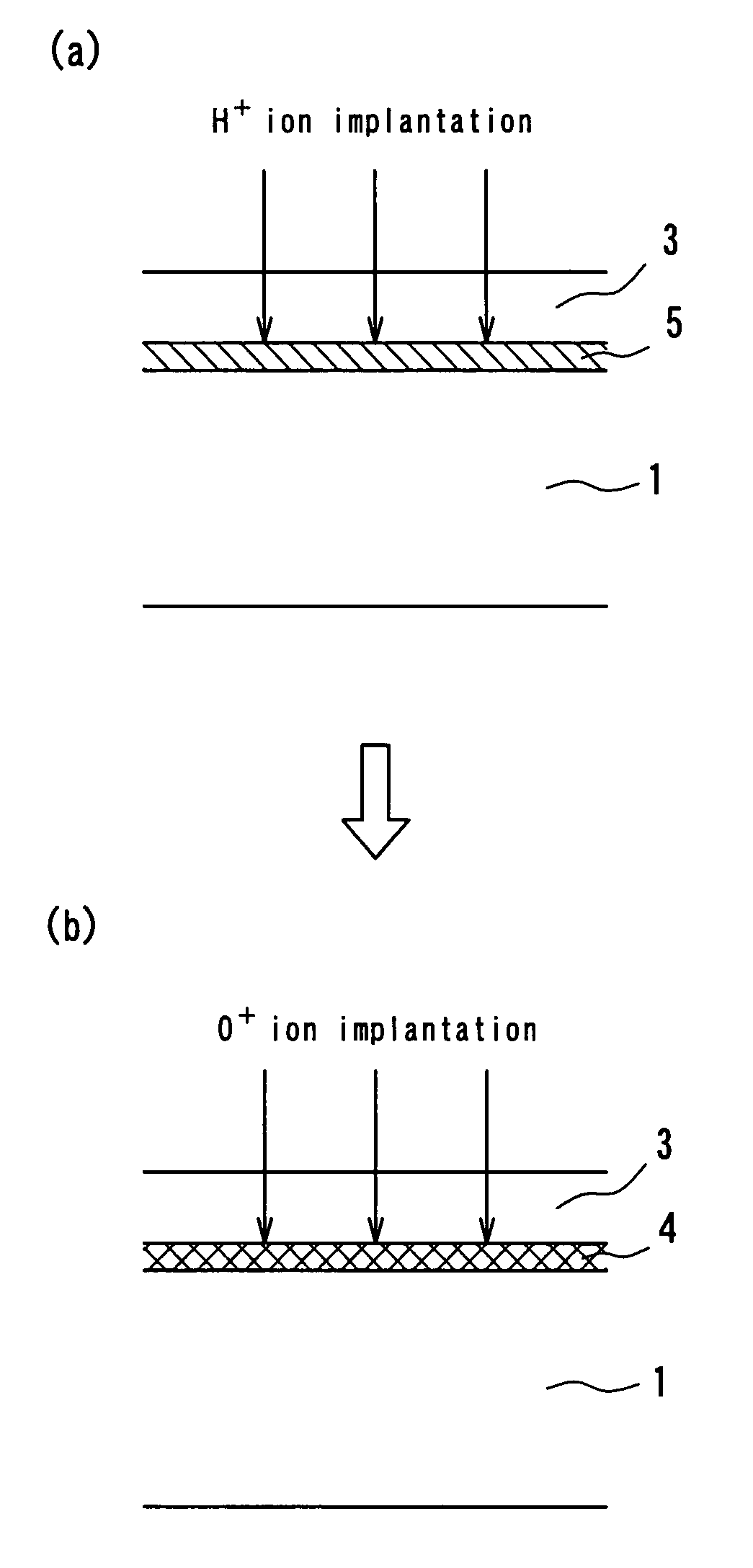
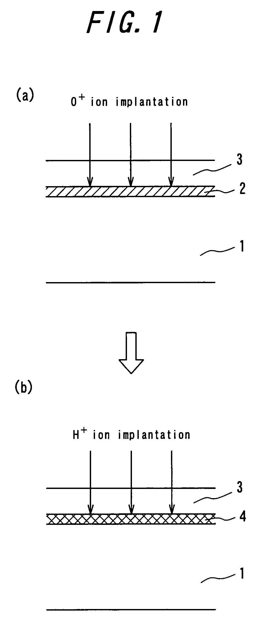
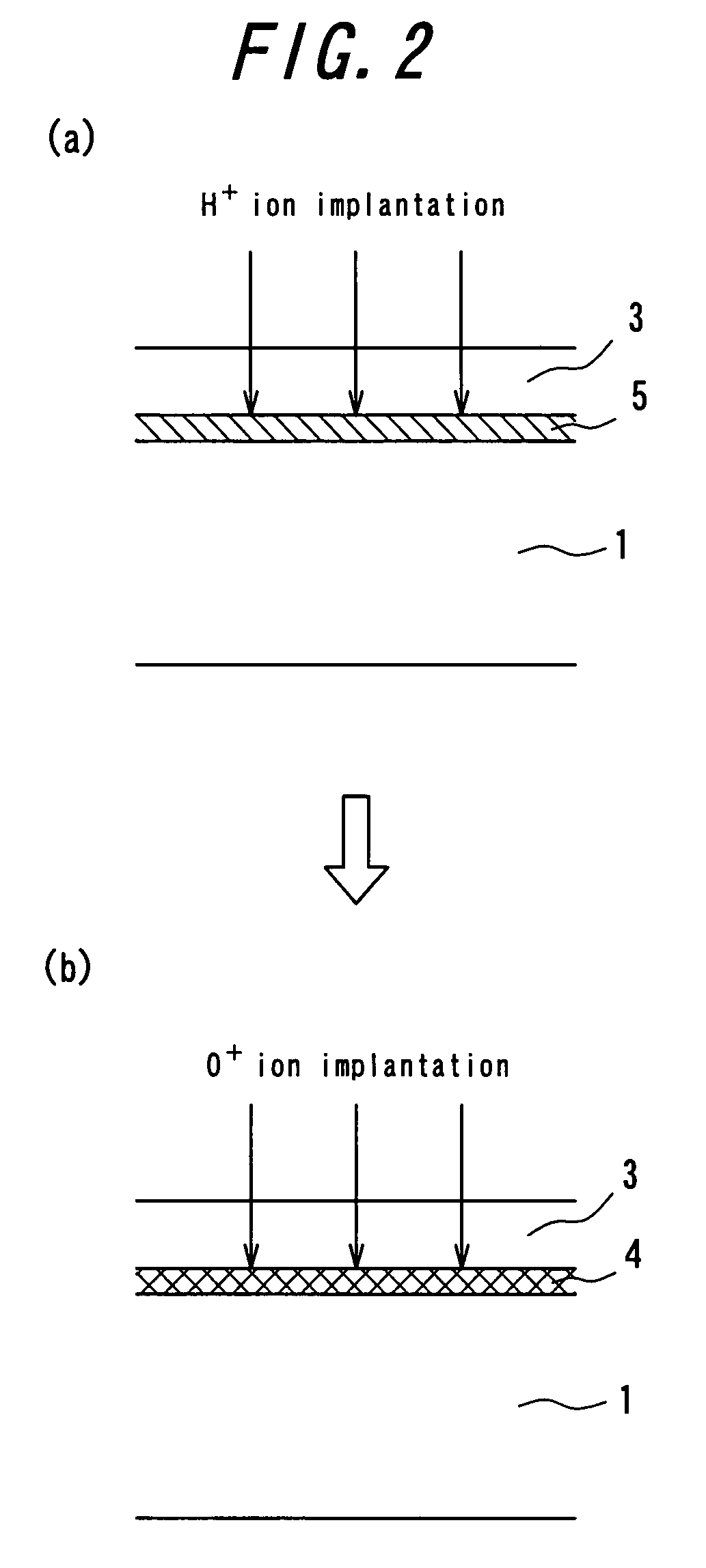
[0012]The inventors have made various studies in order to obtain a sufficient roughness improving effect even in the annealing step at a low temperature for a short time and found that a viscosity of BOX film is lowered by implanting a given dose of hydrogen ion before or after the oxygen ion implantation and that the uniting, growing and flattening of oxygen precipitates are promoted by such a lowering of the viscosity and it is possible to largely improve the roughness in the annealing process at a lower temperature for a shorter time as compared with the conventional technique, and as a result, the invention has been accomplished.
[0020]According to the invention, it is possible to produce a SIMOX wafer in which the surface roughness of SOI and the roughness at the interface between SOI and BOX are improved (or flattened) to a level equal to or more than the conventional ones by implanting a given dose of hydrogen ion before or after the oxygen ion implantation without deteriorating other properties even if the annealing is carried out at a low temperature for a short time.

Problems solved by technology

However, the above conventional SIMOX forming methods have a problem that the annealing step at an extremely high temperature for a long time is required for realizing the roughness improving effect (flattening).

Method used


Image

  • Method of producing SIMOX wafer
  • Method of producing SIMOX wafer
  • Method of producing SIMOX wafer

Examples


invention example

[0036]An embodiment of applying the invention method to the MLD forming method will be explained below;

[0037]FIGS. 3(a), (b) and (c) shows sectional construction of a wafer when the invention method is applied to the MLD forming method, respectively.

[0038]In this method, there are carried out a high-temperature, high dose step wherein an oxygen (16O+) ion is first implanted under conditions of an acceleration energy: 100-250 keV, a dose: (1-10)×1017 / cm2 and a substrate temperature: 200-650° C. and a low-temperature, low dose step wherein the oxygen ion is implanted under conditions of an acceleration energy: 100-250 keV, a dose: (1-10)×1015 / cm2 and a substrate temperature: 20-150° C. (two-stage implantation step).

[0039]Then, a hydrogen (H+) ion is implanted under conditions of an acceleration energy rendering into a position equal to an implantation depth of the oxygen ion, concretely 100-250 keV, a dose: 1015-1017 / cm2 and a substrate temperature: 20-150° C. to form an amorphous lay...


PUM


Abstract

A SIMOX wafer is produced by implanting an oxygen ion, in which a hydrogen ion is implanted at a dose of 1015-1017 / cm2 before or after the step of the oxygen ion implantation.

Description

BACKGROUND OF THE INVENTION[0001]1. Field of the Invention[0002]This invention relates to a thin film SOI wafer having a buried oxide film for forming a high-speed, low power consumption SOI (silicon on insulator) device, and more particularly to a SIMOX (separation by implanted oxygen) wafer in which the buried oxide film is formed by implanting an oxygen ion into a surface of a wafer and then annealing at a high temperature.[0003]2. Description of Related Art[0004]As a method of producing the thin film SOI wafer such as SIMOX wafer, there are known two methods, i.e. a first method is a so-called high-dose SIMOX forming method mainly including a step of implanting a high dose of oxygen ion (16O+), and a second method is a so-called low dose SIMOX forming method including a step of implanting an oxygen ion at a does lower by about one digit than that of the high-dose SIMOX forming method and then annealing in an oxidizing atmosphere having a high oxygen content.[0005]Recently, there...

Claims


Application Information

Patent Timeline
Patent Type & Authority Patents(United States)
IPC IPC(8): H01L21/00
CPCH01L21/26533H01L21/76243H01L21/26593
Inventor MURAKAMI, YOSHIOKO, BONG-GYUN
Owner SUMCO CORP
Learn More