Luminous body, electron beam detector using the same, scanning electron microscope, and mass analysis device

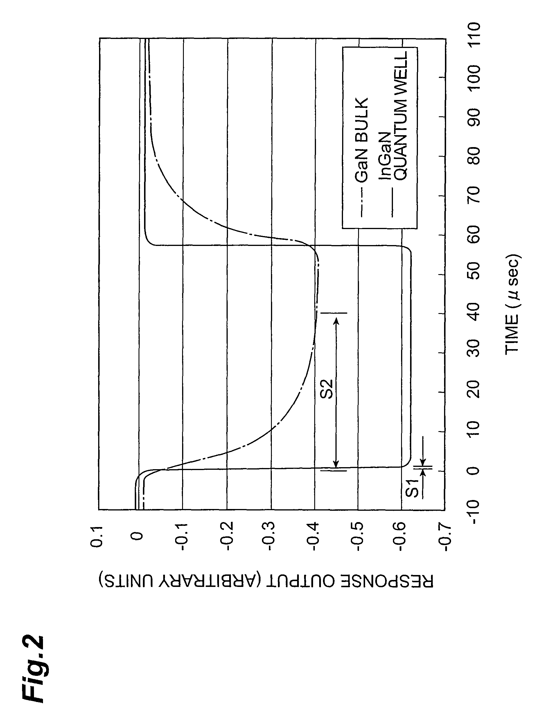
a mass analysis and electron beam technology, applied in the field of luminous bodies, electron beam detectors using the same, scanning electron microscopes, and mass analysis devices, can solve the problems of small charge produced by electron beams, inability to efficiently detect electron beams, and difficulty in obtaining a fast response speed (of the order of sec) sufficient for scanning electron microscopes or mass spectroscopes. achieve the effect of fast response speed

Active Publication Date: 2011-03-22
HAMAMATSU PHOTONICS KK
View PDF19 Cites 18 Cited by
  • Summary
  • Abstract
  • Description
  • Claims
  • Application Information

AI Technical Summary

Benefits of technology

[0006]The present invention was made in order to solve the problem described above, its object being to provide a light-emitting body of fast response speed and high intensity of light emission, and an electron detector, a scanning electron microscope and mass spectroscope using this.

Problems solved by technology

Conventional electron beam detectors, when measuring an electron beam of strong intensity, perform detection of the electron beam by measuring the current value produced by the electron beam, but, in the case of measurement of an electron beam of comparatively low intensity, the amount of charge produced by the electron beam is small, so it is not possible to detect the electron beam efficiently.
However, in the case of a conventional phosphor as shown in FIG. 9, there was the problem that it was difficult to obtain a fast response speed (of the order of μsec) sufficient for a scanning electron microscope or mass spectroscope.
It should be noted that, of the small number of phosphors with which a good response speed is obtained, GaAsP light-emitting bodies have a low intensity of light emission and so were unsuitable for application to scanning electron microscopes and the like.

Method used


Image

  • Luminous body, electron beam detector using the same, scanning electron microscope, and mass analysis device
  • Luminous body, electron beam detector using the same, scanning electron microscope, and mass analysis device
  • Luminous body, electron beam detector using the same, scanning electron microscope, and mass analysis device

Examples


Embodiment Construction

[0042]A mode that is believed to be optimum in implementation of a light-emitting body, and an electron beam detector, a scanning electron microscope and mass spectroscope using this according to the present invention are described below in detail with reference to the appended drawings. Elements which are the same or similar are indicated by the same reference symbols and where the description would be duplicated such description is dispensed with.

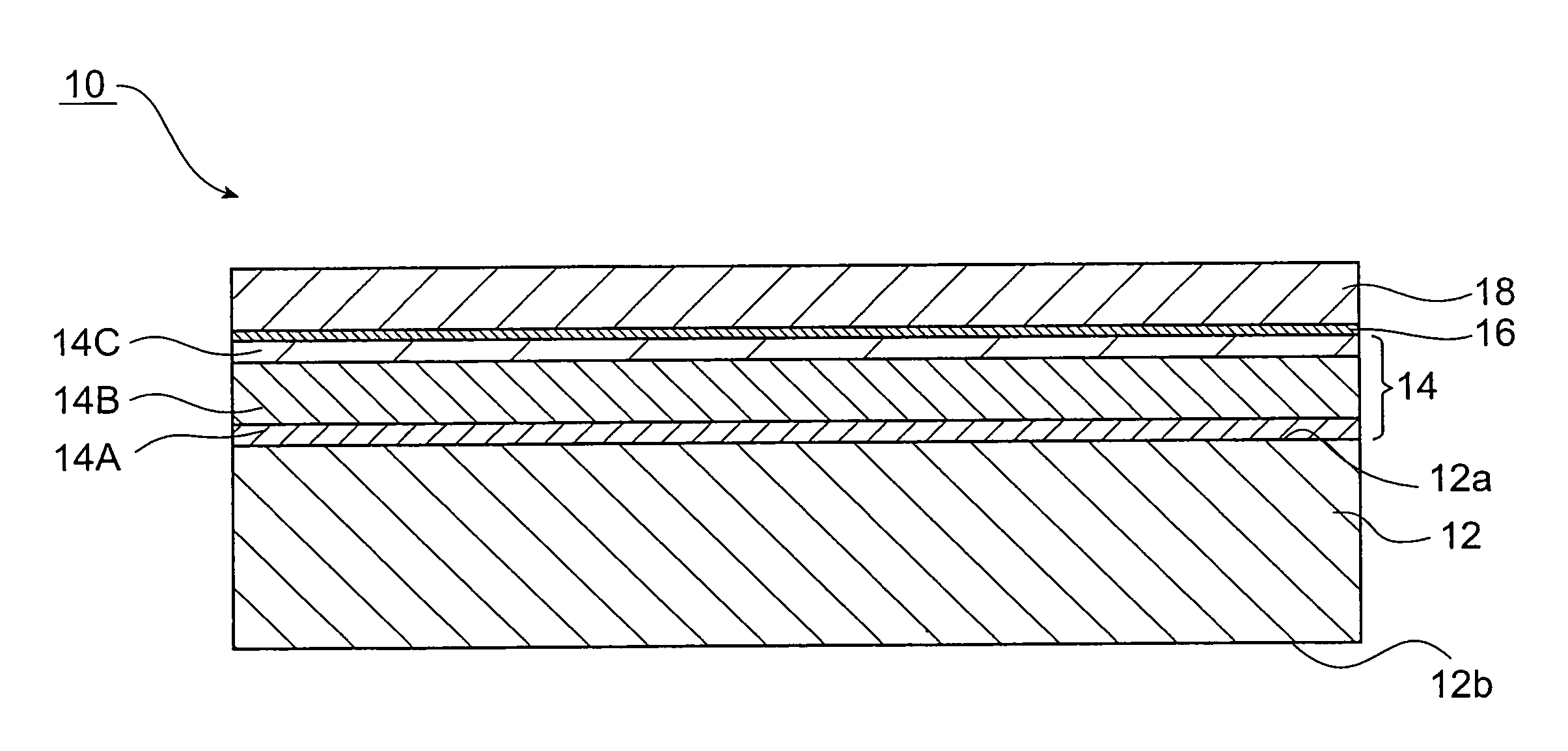
[0043]As shown in FIG. 1, a light-emitting body 10 comprises a base 12, a nitride semiconductor layer 14 formed on the substrate surface 12a, a cap layer 16 and metal backing layer (reflective film) 18 successively laminated on the nitride semiconductor layer 14. Attracted by the positive potential applied to the metal backing layer 18, electrons are directed onto the metal backing layer 18. Since the metal backing layer 18 has a thickness capable of transmitting electrons, electrons are incident on the interface (electron incidence face)...


PUM

PropertyMeasurementUnit
thicknessaaaaaaaaaa
well widthaaaaaaaaaa
thicknessaaaaaaaaaa

Abstract

A light-emitting body of rapid speed of response and high light emission intensity, and an electron beam detector, scanning electron microscope and mass spectroscope using this are provided. In the light-emitting body 10 according to the present invention, when fluorescence is emitted by a nitride semiconductor layer 14 formed on one face 12a of a substrate 12 in response to incidence of electrons, at least some of this fluorescence is transmitted through this substrate 12, whereby that fluorescence is emitted from the other face 12b of the substrate. The response speed of this fluorescence is not more than μsec order. Also, the intensity of emission of this fluorescence is almost identical to that of a conventional P47 phosphor. Specifically, with this light-emitting body 10, a response speed and light emission intensity are obtained that are fully satisfactory for application to a scanning electron microscope or mass spectroscope. In addition, a cap layer 16 contributes to improvement in the persistence rate of light emission in the nitride semiconductor layer 14, so, with this light-emitting body 10, not only high-speed response and high light emission intensity are obtained, but also an excellent persistence rate.

Description

TECHNICAL FIELD[0001]The present invention relates to a light-emitting body that emits light in response to incidence of electrons, an electron beam detector, a scanning electron microscope and a mass spectroscope using the light-emitting body.BACKGROUND ART[0002]Conventional electron beam detectors, when measuring an electron beam of strong intensity, perform detection of the electron beam by measuring the current value produced by the electron beam, but, in the case of measurement of an electron beam of comparatively low intensity, the amount of charge produced by the electron beam is small, so it is not possible to detect the electron beam efficiently. Accordingly, in the case of an electron beam detector used in for example a scanning electron microscope (SEM), measurement is conducted by irradiating a sample surface with the electron beam, collecting the secondary electrons generated at this sample surface and using these to irradiate a phosphor, and detecting the fluorescence ...

Claims


Application Information

Patent Timeline
Patent Type & Authority Patents(United States)
IPC IPC(8): H01J49/02G01N23/225C09K11/62G01N27/62G01T1/20G01T1/29H01J37/244H01J49/06H01J49/10
CPCH01J37/244H01J49/025H01J2237/2443H01L33/502
Inventor UCHIYAMA, SHOICHITAKAGI, YASUFUMINIIGAKI, MINORUKONDO, MINORUMIZUNO, ITARU
Owner HAMAMATSU PHOTONICS KK
Why Eureka
Try Eureka