Inductive coupling for communications equipment interface circuitry

a communication equipment and interface circuit technology, applied in the field of high-voltage electrical interfaces, can solve the problems of limited success in rejecting high-voltage common-mode signals, high-voltage common-mode signals such as 20-volt peak-to-peak, capacitors capable of withstanding high-voltage common-mode signals, and high-voltage common-mode signals, etc., to achieve the effect of improving attenuation

Inactive Publication Date: 2011-03-22
AVAGO TECH INT SALES PTE LTD
View PDF27 Cites 5 Cited by
  • Summary
  • Abstract
  • Description
  • Claims
  • Application Information

AI Technical Summary

Benefits of technology

[0010]Other aspects of the invention provide for an input attenuation element coupled to one of the signal paths forming the input differential signal pair. The input attenuation element can act as a high-pass filter. Further features of the invention can also provide for a low-pass filter that attenuates an undesired signal in the output differential signal pair. Additional aspects of the invention also provide for a high-pass filter and a low-pass filter having overlapping cut-off frequencies that thereby provide for improved noise immunity.
[0012]The invention also includes a method for interfacing an input differential signal pair to an output differential signal pair. In particular, the method includes the steps of inductively coupling the input differential signal pair to an output differential signal pair, and filtering out a common mode signal occurring in the output differential signal pair. The inventive method improves the attenuation of an undesired signal found in a differential signal path by using inductive coupling.

Problems solved by technology

Capacitive coupling, however, has limited success in rejecting high voltage (e.g. 20 volts peak-to-peak) common mode signals.
Capacitors capable of withstanding high voltage common mode signals, such as a 0.01 micro-Farad, 3 kilo-volt rated capacitor, are both expensive and bulky.
Furthermore, known capacitive coupling techniques are unable to reject high voltage signals over a broad frequency range.
Any common mode noise signals over this broad frequency range which are not attenuated will push the transmitted signals into ground or into the chip voltage rail, thereby corrupting the transmitted data.

Method used


Image

  • Inductive coupling for communications equipment interface circuitry
  • Inductive coupling for communications equipment interface circuitry
  • Inductive coupling for communications equipment interface circuitry

Examples


Embodiment Construction

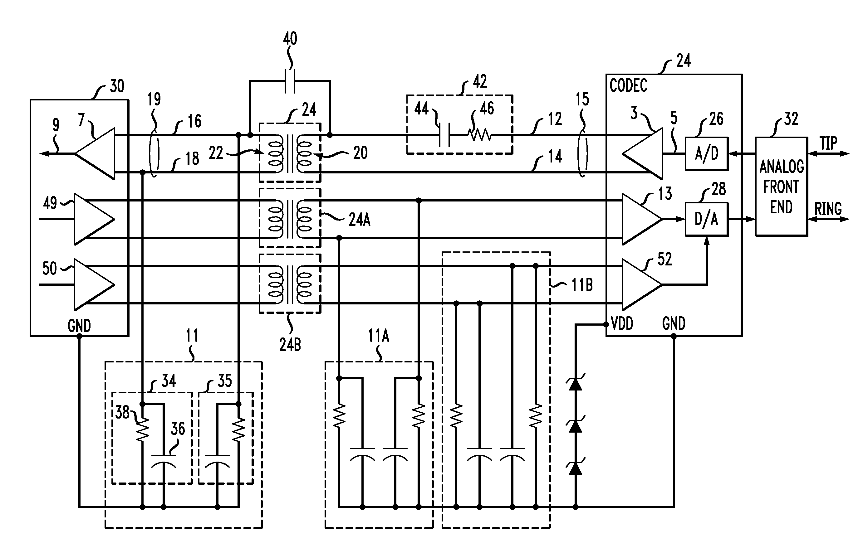
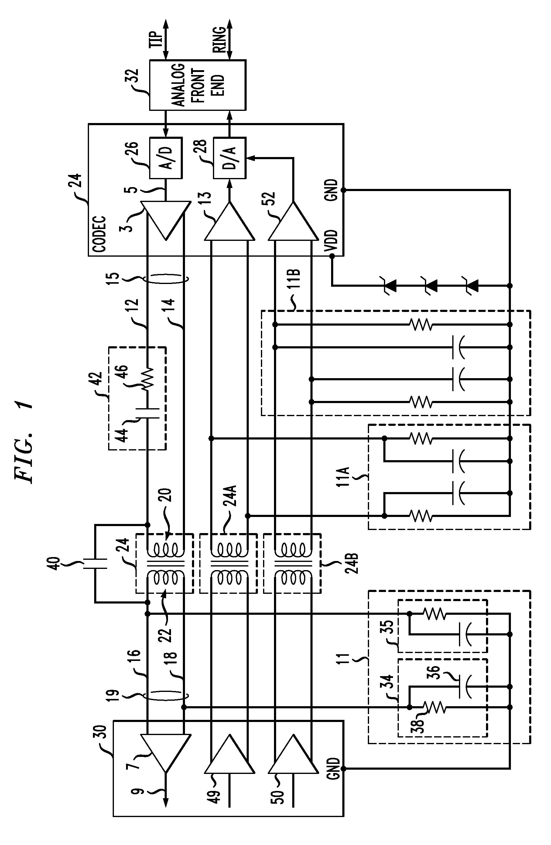
[0017]FIG. 1 is a mixed block and schematic diagram of an electrical interface 10 in accordance with the present invention. The electrical interface includes a primary inductor 20 and a secondary inductor 22 for operably coupling an input differential signal pair 15 to an output differential signal pair 19. The interface 10 also includes a filter 11 that attenuates a signal occurring in the output differential signal pair 19.

[0018]The primary inductor 20 and the secondary inductor 22 inductively couple the input differential signal pair 15 to the output differential signal pair 19. The inductive coupling also electrically isolates a digital circuit 30 from the TIP and RING contacts of the telephone lines. The electrical isolation function of the primary and secondary inductors prevent telephone equipment from applying voltage surges or ground connections to the telephone lines, and vice versa. The filter 11, in accordance with the invention, attenuates common mode noise signals in t...


PUM


Abstract

A system for improving the attenuation of an undesired signal found in a differential signal path through the use of inductive coupling. The system includes a primary inductor, a secondary inductor, and a filter. The primary inductor and the secondary inductor operably couple an input differential signal pair to an output differential signal pair, and the filter attenuates an undesired signal in the output differential signal pair.

Description

REFERENCE TO RELATED APPLICATIONS[0001]This application is a continuation of co-pending U.S. patent application Ser. No. 09 / 723,451 filed on Nov. 28, 2000, which is a continuation-in-part of U.S. patent application Ser. No. 09 / 605,953 filed on Jun. 28, 2000 and issued as U.S. Pat. No. 7,113,587 on Sep. 26, 2006, the contents of both of which are incorporated herein by reference in their entirety.FIELD OF THE INVENTION[0002]This invention relates to an electrical interface. Specifically, the invention proposes a high-voltage electrical interface with improved noise performance.BACKGROUND OF INVENTION[0003]A conventional solution to noise degradation is to use a differential mode of signaling. In differential signaling, a single data signal is transmitted over two wires (e.g. first and second signal lines), each of which carries one signal component. The two components are generally derived from the same source data signal and are varied such that the data signal is transmitted as the...

Claims


Application Information

Patent Timeline
Patent Type & Authority Patents(United States)
IPC IPC(8): H04M1/00H03H7/00H03K19/0175H04B3/03H04L25/02H04M11/06
CPCH04L25/0266H04M11/06H03H7/00
Inventor FUEHRER, TIMOTHY W.LATURELL, DONALD R.SMITH, LANE A.WITTENSOLDNER, CHRISTOPHER J.
Owner AVAGO TECH INT SALES PTE LTD
Why Eureka
Try Eureka