Testing an embedded core

a technology of embedded cores and cores, applied in the direction of electronic circuit testing, measurement devices, instruments, etc., can solve the problems of inability to instantiate, fpga may pose a problem for testing,

Active Publication Date: 2011-03-29
XILINX INC
View PDF6 Cites 26 Cited by
  • Summary
  • Abstract
  • Description
  • Claims
  • Application Information

AI Technical Summary

Benefits of technology

[0013]Another aspect relates generally to a system for testing an embedded core coupled to an array of memory cells within a host IC. The system includes a programmed computer which is programmed with a testing software program. A device under test is coupled to the programmed computer for receiving test vectors therefrom and for providing test results thereto responsive to the test vectors. The device under test includes a write controller for respectively receiving portions of the test vectors and configured to convert each portion of the portions from serial to parallel to output data. The write controller is configured to generate control information and address information. A memory controller is coupled to the write controller for receiving the address information, the control information, and the data therefrom. The array of memory cells is coupled to the memory controller, the memory controller for selectively writing the data to locations in the array of memory cells. The embedded core is coupled to the array of memory cells, wherein operation of the embedded core is dynamically alterable responsive to the data input from the array of memory cells. The write controller, the memory controller, and the array of memory cells are configured to mimic scan chain input with respect to the testing software for testing the embedded core.
[0014]Yet another aspect relates generally to a host IC having an embedded core and memory. The host IC has a write controller for respectively receiving portions of test vectors. A memory controller is coupled to the write controller for receiving address information, control information, and data from the write controller. The memory is coupled to the memory controller for selectively writing the data thereto. The embedded core is coupled to the memory, wherein operation of the embedded core and the memory is configured for dynamically writing to the memory while operating the embedded core. The write controller, the memory controller, and the memory are configured to mimic scan chain input with respect to a testing software program for testing the embedded core.

Problems solved by technology

However, one or more hardwired embedded cores (“embedded core”) in an FPGA may pose a problem for testing.
For example, an embedded core manufactured as part of an FPGA may have some or all of its interface pins, which would be accessible if such core were manufactured as a standalone device, generally not readily accessible other than via circuitry of the FPGA.
In other words, such scan chain overhead may not be included as part of the integrated circuit, or, in the example of PLDs, may not be capable of being instantiated for being directly coupled to such interface portion.
Unfortunately, software test benches used to generate test patterns for testing ICs operate under the assumption of a scan chain input for providing test vectors to test circuits.

Method used


Image

  • Testing an embedded core
  • Testing an embedded core
  • Testing an embedded core

Examples


Embodiment Construction

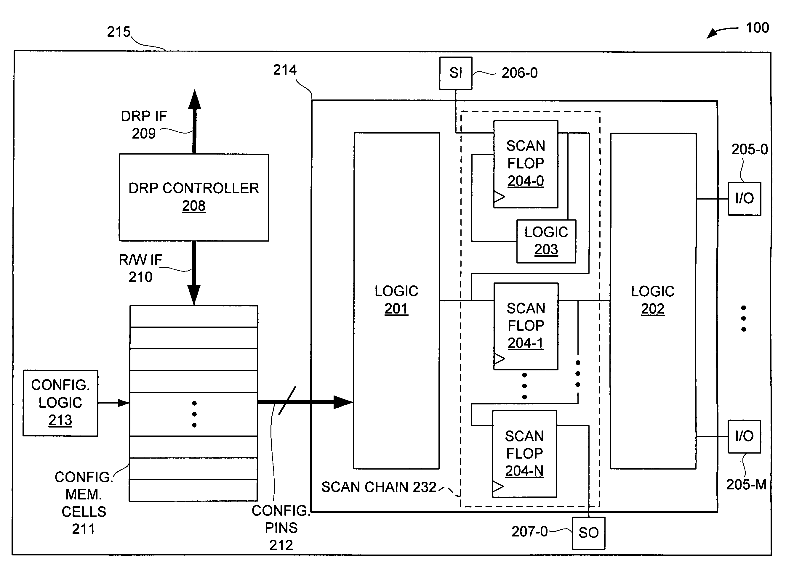
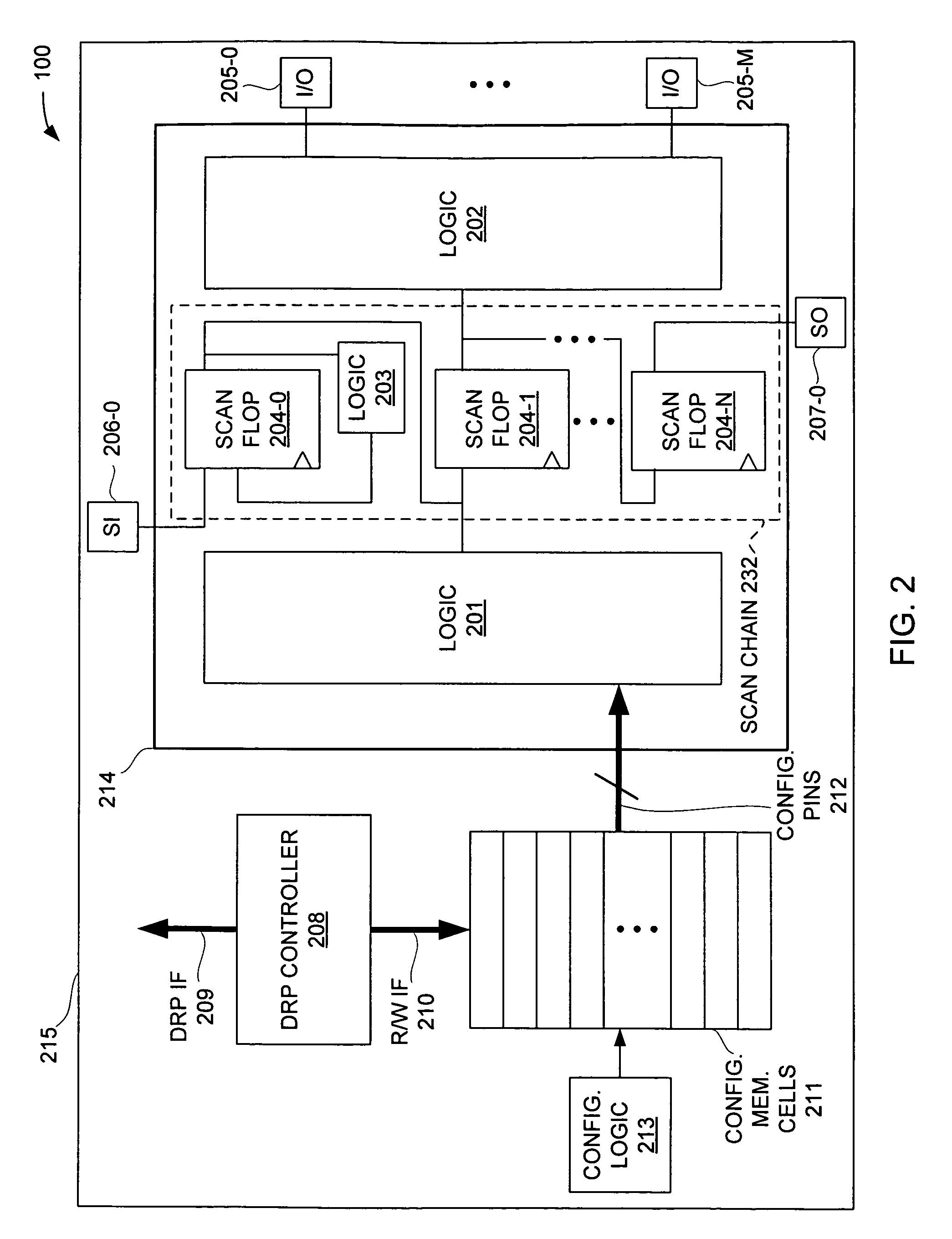
[0023]In the following description, numerous specific details are set forth to provide a more thorough description of the specific embodiments of the invention. It should be apparent, however, to one skilled in the art, that the invention may be practiced without all the specific details given below. In other instances, well known features have not been described in detail so as not to obscure the invention. For ease of illustration, the same number labels are used in different diagrams to refer to the same items; however, in alternative embodiments the items may be different.

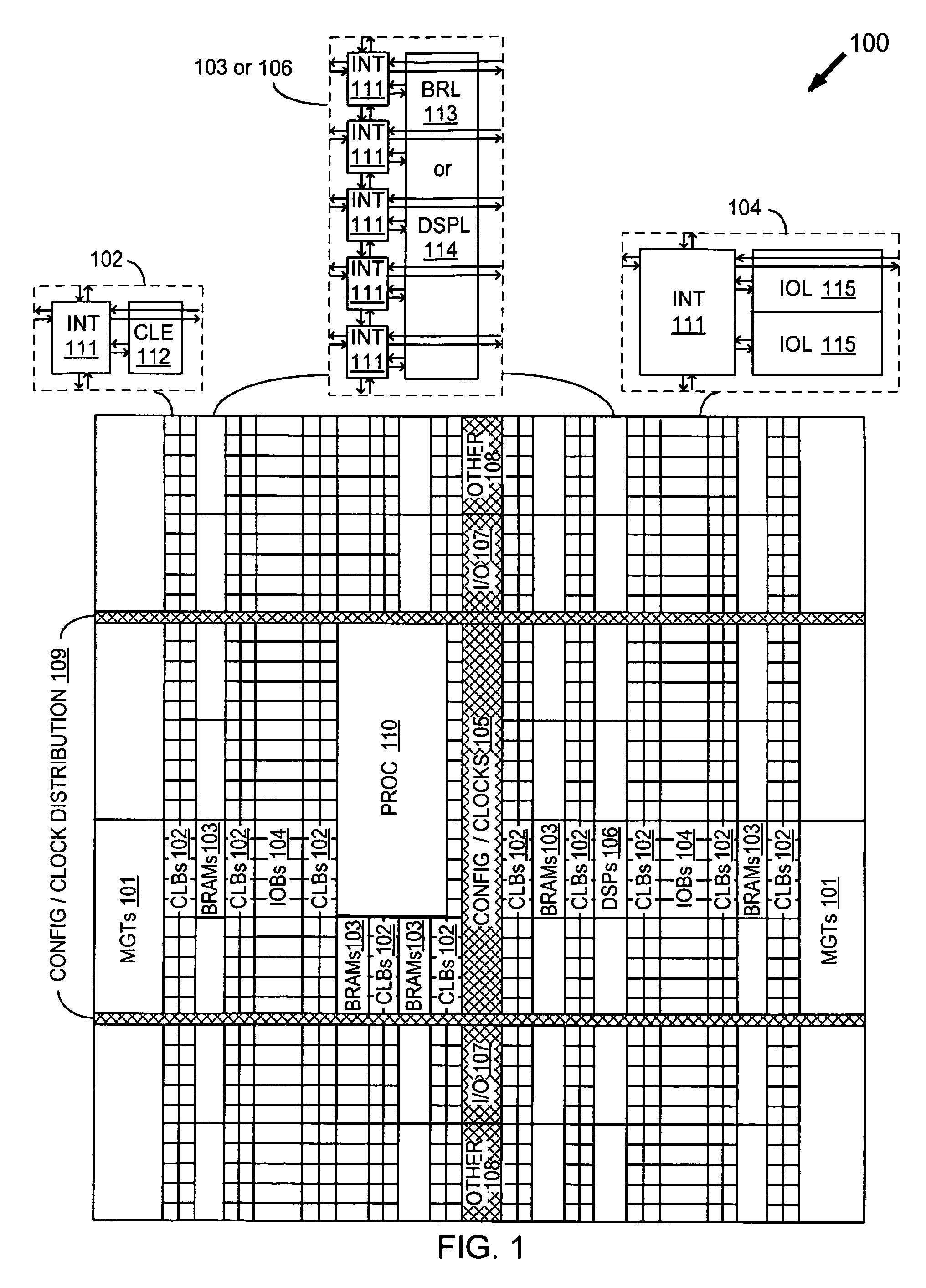
[0024]FPGAs can include several different types of programmable logic blocks in the array. For example, FIG. 1 illustrates an FPGA architecture 100 that includes a large number of different programmable tiles including multi-gigabit transceivers (“MGTs”) 101, configurable logic blocks (“CLBs”) 102, random access memory blocks (“BRAMs”) 103, input / output blocks (“IOBs”) 104, configuration and clocking logic (“CO...


PUM


Abstract

A method of testing of an embedded core of an integrated circuit (“IC”) is described. An IC has a hardwired embedded core and memory coupled to each other in the IC. The method includes writing a test vector to the memory while the embedded core is operative. The test vector is input from the memory to the embedded core to mimic scan chain input to the embedded core. A test result is obtained from the embedded core responsive in part to the test vector input.

Description

FIELD OF THE INVENTION[0001]The invention relates to integrated circuit devices (ICs). More particularly, the invention relates to testing an embedded core of an IC.BACKGROUND OF THE INVENTION[0002]Programmable logic devices (“PLDs”) are a well-known type of integrated circuit that can be programmed to perform specified logic functions. One type of PLD, the field programmable gate array (“FPGA”), typically includes an array of programmable tiles. These programmable tiles can include, for example, input / output blocks (“IOBs”), configurable logic blocks (“CLBs”), dedicated random access memory blocks (“BRAMs”), multipliers, digital signal processing blocks (“DSPs”), processors, clock managers, delay lock loops (“DLLs”), and so forth. As used herein, “include” and “including” mean including without limitation.[0003]Each programmable tile typically includes both programmable interconnect and programmable logic. The programmable interconnect typically includes a large number of interconn...

Claims


Application Information

Patent Timeline
Patent Type & Authority Patents(United States)
IPC IPC(8): G01R31/28
CPCG01R31/318597G11C29/32G11C2029/0401G11C2029/3202
Inventor PAVLE, ADARSHTOUTOUNCHI, SHAHIN
Owner XILINX INC
Why Eureka
Try Eureka