

Integrated circuit packaging method with postpositional embedded core flow and package structure
A technology of integrated circuits and packaging methods, which is applied in the direction of circuits, electrical components, and electric solid devices, and can solve the problems of reduced compactness of integrated circuits, increased manufacturing process steps, and reduced production yields, so as to improve the heat dissipation performance of chips and simplify The production process and the effect of improving electrical performance
- Summary
- Abstract
- Description
- Claims
- Application Information
AI Technical Summary
Problems solved by technology
Method used
Image

Examples
Embodiment 1
[0075] This embodiment provides an integrated circuit packaging method and its corresponding packaging structure after the buried core process.
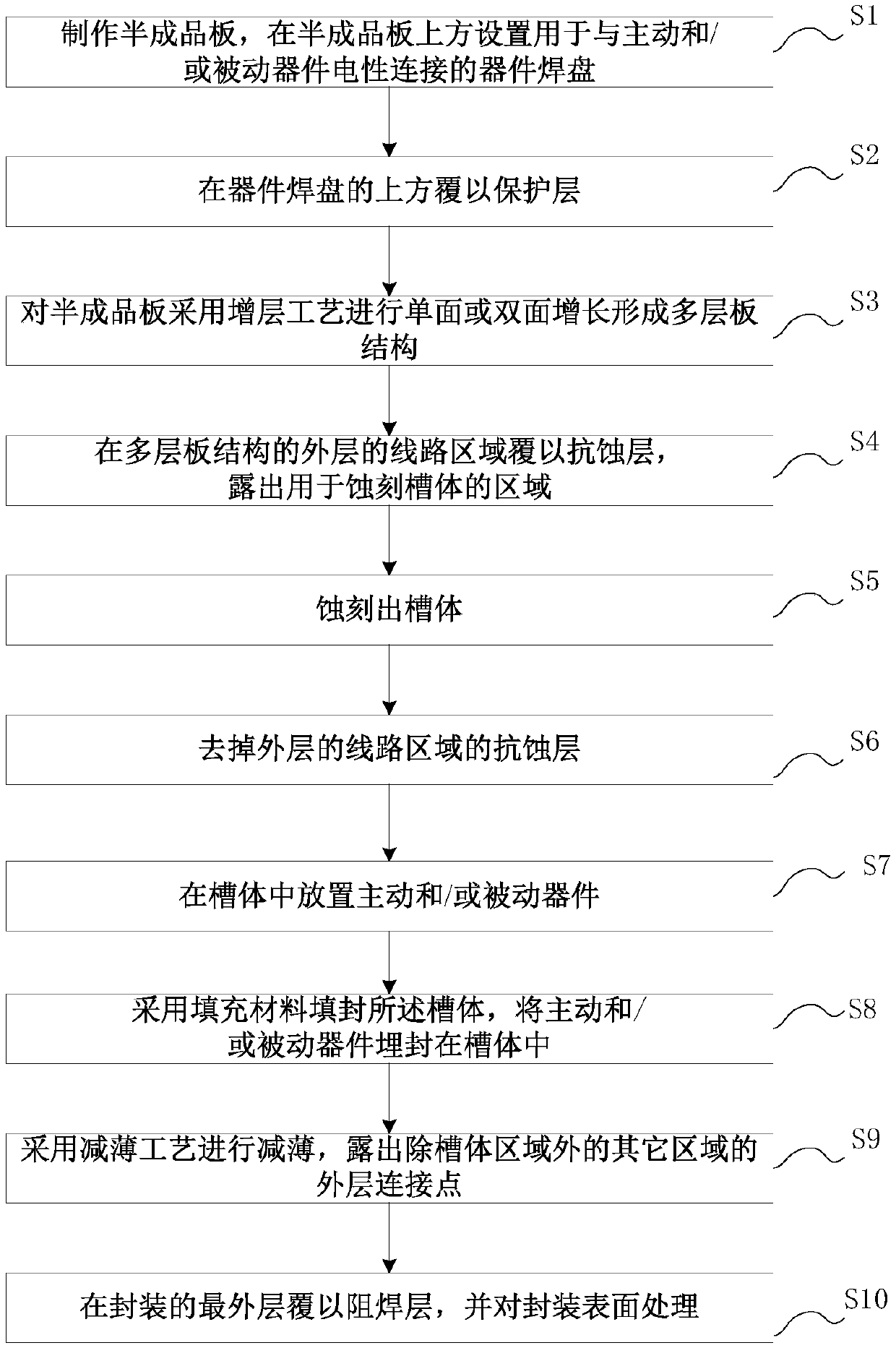
[0076] In this example, if figure 1 As shown, a post-buried integrated circuit packaging method includes the following steps:
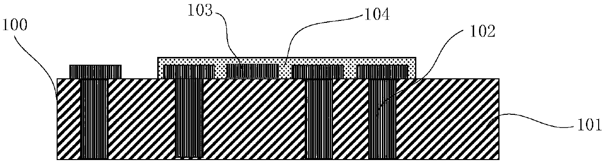
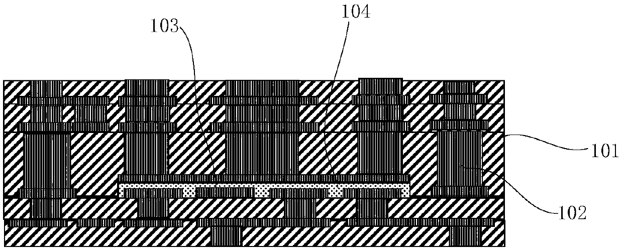
[0077] S1 , making a semi-finished board 100 , and disposing device pads 103 for electrically connecting active and / or passive devices 200 on the semi-finished board 100 . In the packaging method of the present invention, the semi-finished board 100 is first produced. The semi-finished board 100 is generally a packaging structure located under the active and / or passive device 200. The semi-finished board 100 can be a single-layer board structure or a multi-layer board structure. Such as figure 2 As shown, the semi-finished board 100 of this embodiment is a single-layer board structure, including a packaging material 101, and the packaging material 101 is provided with conductive copper pillars 102 (electr...
Embodiment 2
[0112] This embodiment provides an integrated circuit packaging method and a corresponding packaging structure after the component embedding process.
[0113] In this example, if Figure 10 As shown, the integrated circuit packaging method after the component embedding process includes the following steps:
[0114]P1 , making a semi-finished board 100 , and disposing device pads 103 for electrically connecting active and / or passive devices 200 on the semi-finished board 100 . In the packaging method of the present invention, the semi-finished board 100 is first produced. The semi-finished board 100 is generally a packaging structure located under the active and / or passive device 200. The semi-finished board 100 can be a single-layer board structure or a multi-layer board structure. Such as Figure 11 As shown, the semi-finished board 100 of this embodiment is a single-layer board structure, including a packaging material 101, and the packaging material 101 is provided with c...
PUM
 Abstract
Description
Claims
Application Information