Semiconductor lighting device with reflective remote wavelength conversion

Inactive Publication Date: 2011-04-12
LEDNOVATION
View PDF10 Cites 268 Cited by
  • Summary
  • Abstract
  • Description
  • Claims
  • Application Information

AI Technical Summary

Benefits of technology

[0027]An object of the present invention is to suppress phosphor converting back-scattering loss and phosphor degradation issues of known phosphor-converted (PC) semiconductor lighting devices by utilizing a reflective remot

Problems solved by technology

Current state-of-the-art phosphor-converted LED (Pc-LED) technology is inefficient due to backscattering issues.
But, the back-transferred primary short wavelength radiation and back-transferred down-converted radiation will primari

Method used


Image

  • Semiconductor lighting device with reflective remote wavelength conversion
  • Semiconductor lighting device with reflective remote wavelength conversion
  • Semiconductor lighting device with reflective remote wavelength conversion

Examples


Embodiment Construction

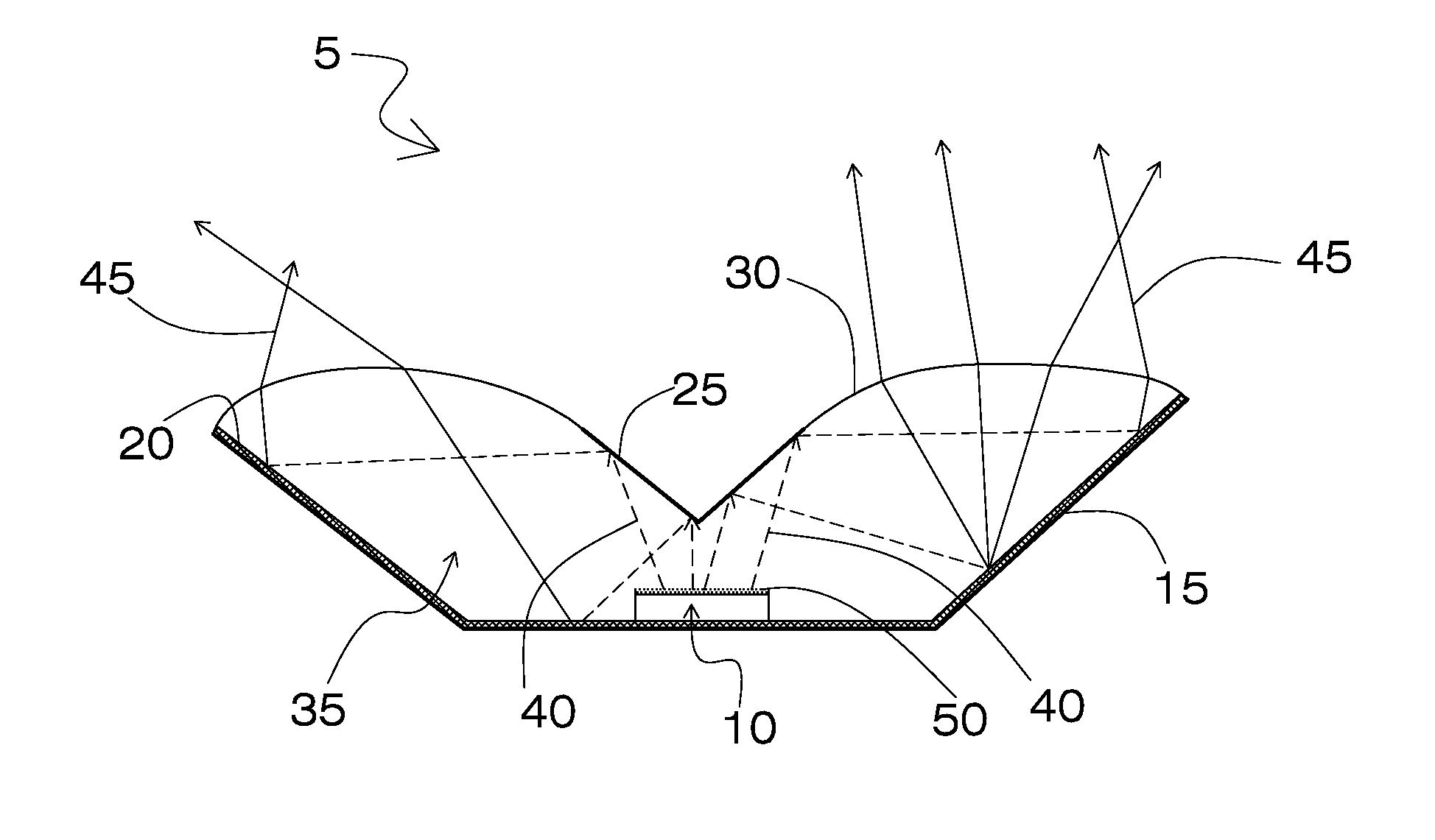
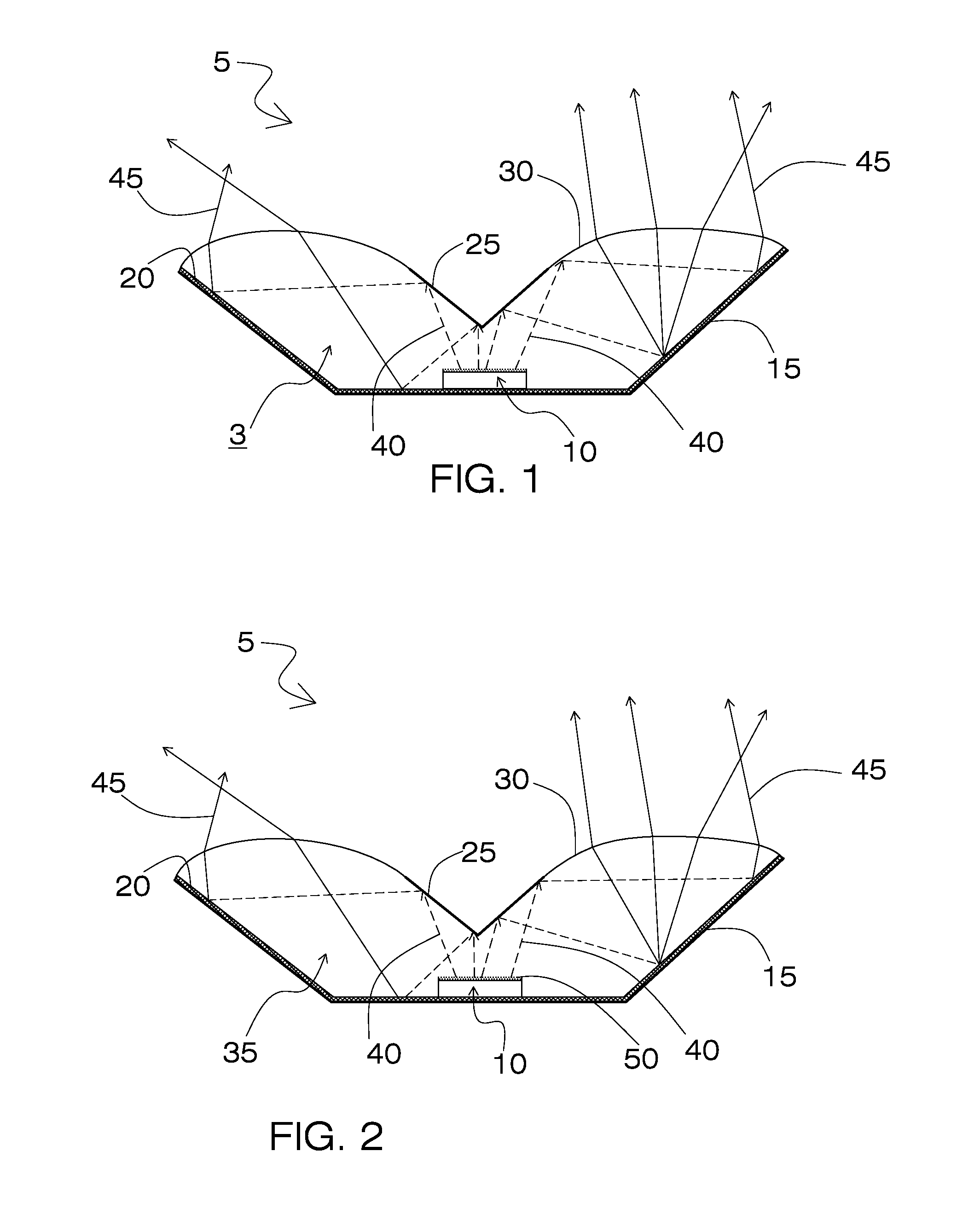
[0036]Referring now to FIG. 1, it will be seen that an illustrative embodiment of the invention is denoted as a whole by the reference numeral 5.

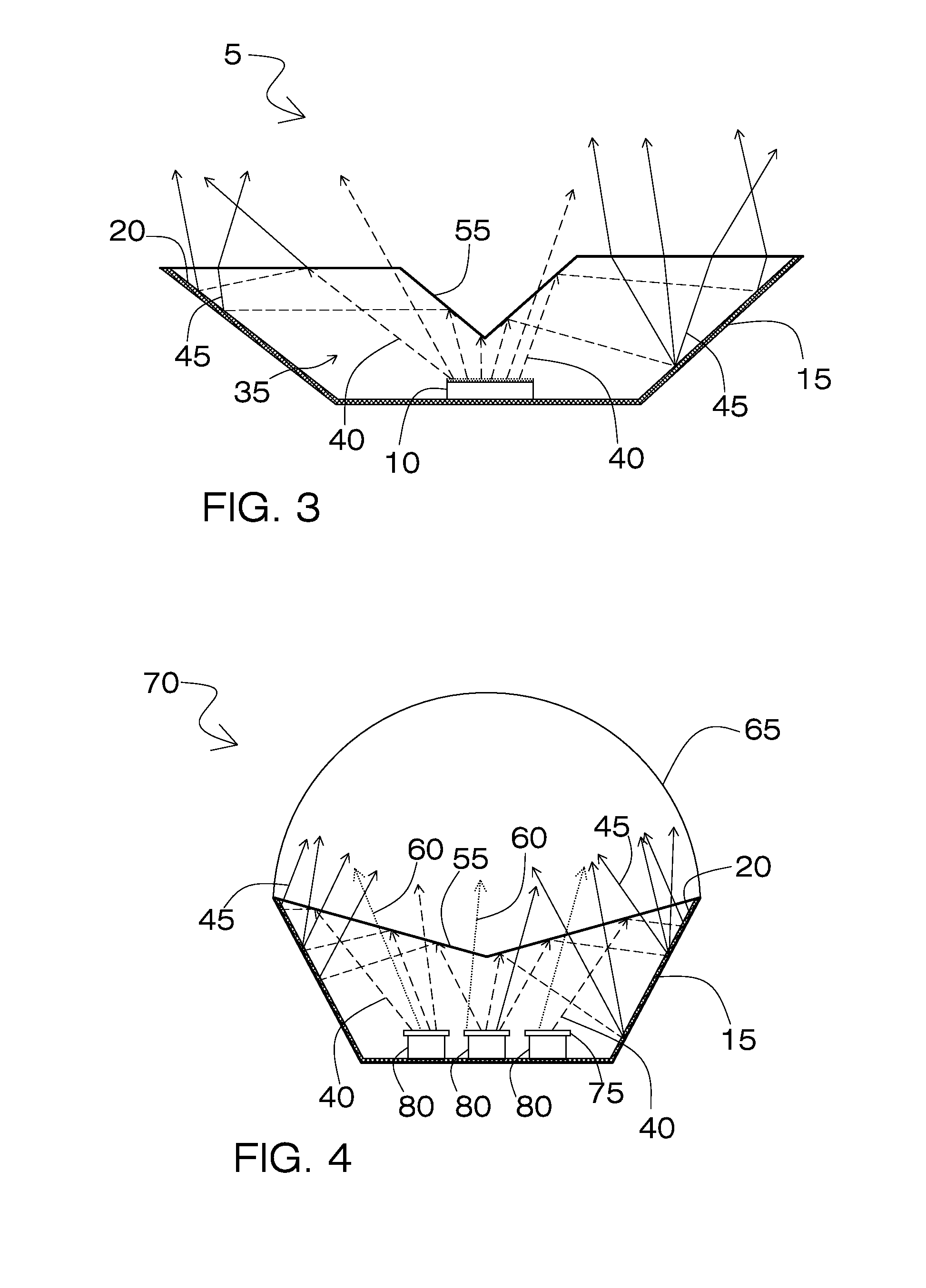
[0037]In the embodiment of FIG. 1, semiconductor white light emitting device 5 includes at least one semiconductor light emitting element 10 and a remote wavelength conversion layer 20 deposited on a reflective interior surface of a wavelength conversion cavity 15. A high refractive index encapsulation material 35 is positioned to substantially fill the wavelength conversion cavity, thereby forming a light extraction surface 30 at the interface between the encapsulation material 35 and the air. The semiconductor light emitting device 5 further includes a deflector element 25 positioned within the encapsulation material 35 at the light extraction surface 30 and in a primary light emitting forward path of the semiconductor light emitting element 10.

[0038]In FIG. 1, the semiconductor white lighting device 5 comprises at least one semiconductor...


PUM


Abstract

A semiconductor lighting device includes at least one semiconductor light emitter and at least one wavelength converting element, physically separated from the light emitter. At least one wavelength converting element has a reflective member underneath it, so that both primary light and converted light from the wavelength converting layer become a forward transferred light preventing from backscattering loss into the light emitter. The reflective member may be a thermal conductive element to effectively remove the heat from the wavelength converting element. Accordingly, the remote wavelength conversion on a reflective surface improves the thermal stability of the wavelength conversion material and prevents backscattering loss to produce a higher radiance result from the device.

Description

BACKGROUND OF THE INVENTION[0001]1. Field of the Invention[0002]The invention relates generally to semiconductor lighting devices, as well as related components, systems and methods, and more particularly to a method of remote wavelength conversion to produce white light from a semiconductor light emitter.[0003]2. Background of the Invention[0004]A typical semiconductor light emitting device utilizes a blue light emitting diode (LED) having a main emission peak in blue wavelength range from 400 nm to 490 nm, and a luminescent layer containing an inorganic phosphor that absorbs blue light emitted by the blue LED and produces an exciting light having an emission peak in a visible wavelength range from green to yellow. The mixture of emitted blue light and excited yellow light produces a white light with correlated color temperature (CCT) around 6500K.[0005]Light emitting semiconductor devices known in the art place a phosphor layer in the light emitting path of the light emitting diod...

Claims


Application Information

Patent Timeline
IPC IPC(8): H01L33/60
CPCH01L33/60H01L33/54H01L25/0753H01L33/50H01L2924/0002H01L2924/00
Inventor ZHAI, JINHUIMOREJON, ISRAEL J.
Owner LEDNOVATION
Why Eureka
Try Eureka