

Thin-film crystal wafer having pn junction and method for fabricating the wafer
a thin-film crystal wafer and pn junction technology, which is applied in the direction of semiconductor devices, electrical apparatus, transistors, etc., can solve the problems of severe limitations in the hbt system, defects at the interface, and inability to achieve electrical characteristics suitable for the requirements. to achieve the effect of inhibiting
- Summary
- Abstract
- Description
- Claims
- Application Information
AI Technical Summary
Benefits of technology
Problems solved by technology
Method used
Image

Examples
Embodiment Construction
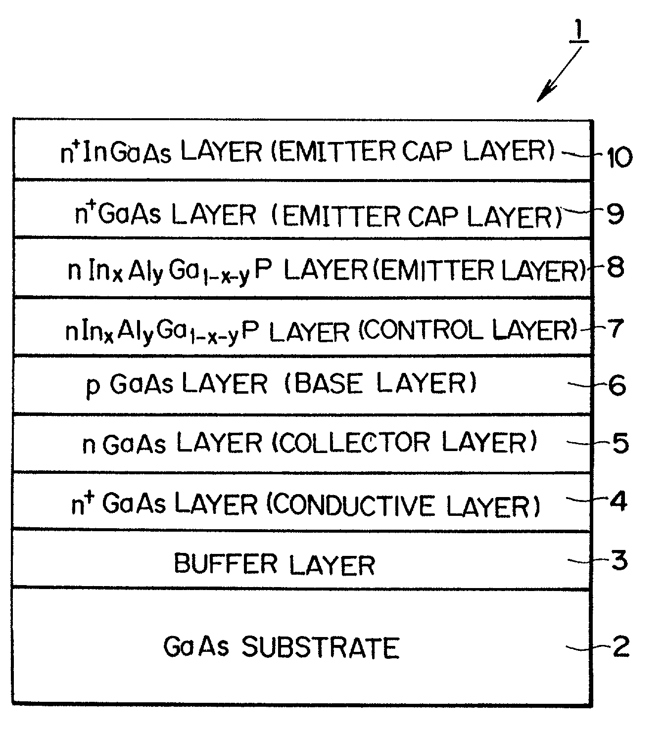
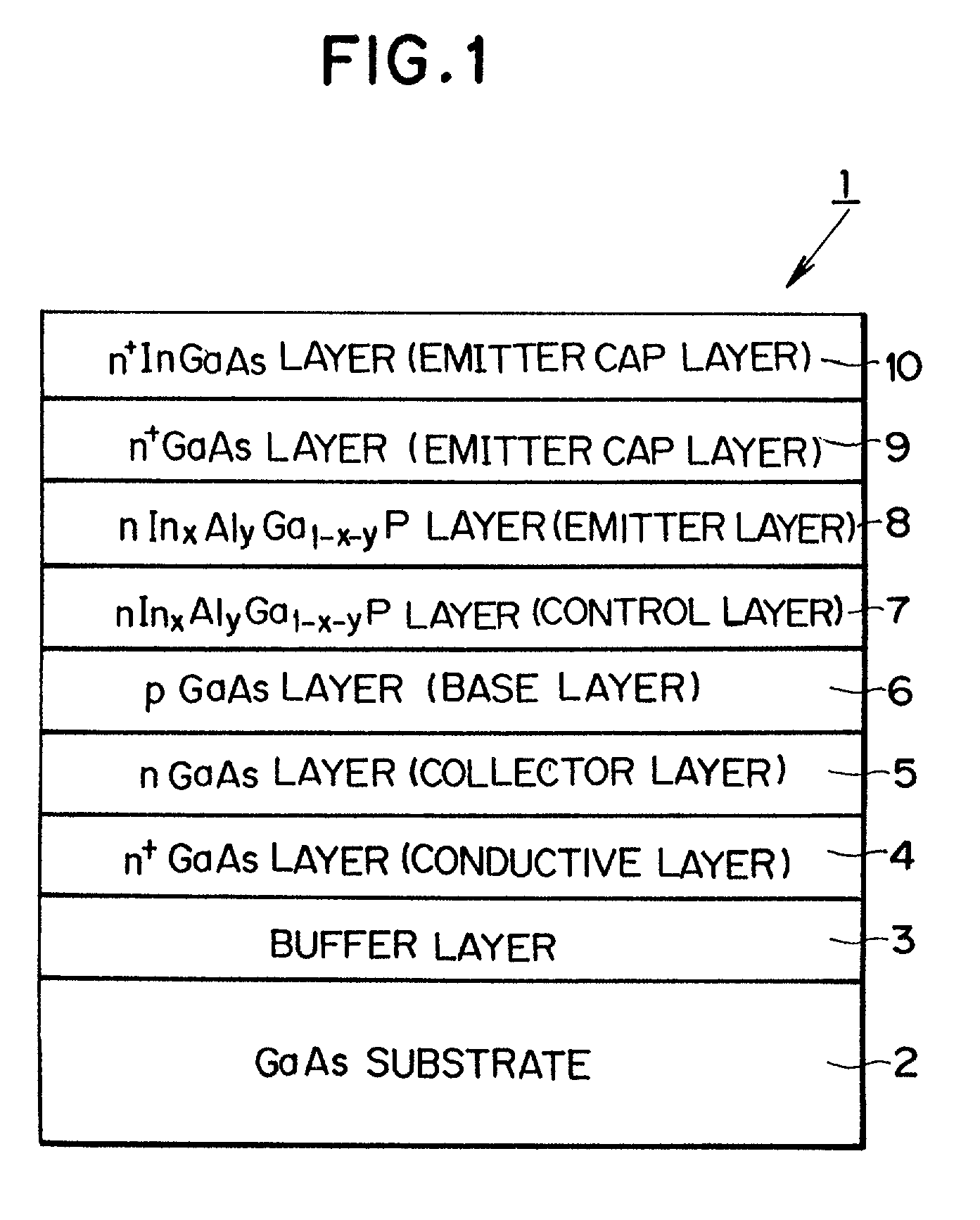
[0024]FIG. 1 is a schematic sectional view of a thin-film crystal wafer having a pn junction that is an embodiment of the present invention. The thin-film crystal wafer 1, which is used to fabricate an HBT, has a multilayer structure consisting of semiconductor thin-film crystal layers successively overlaid on a GaAs substrate 2 composed of semi-insulating GaAs compound semiconductor crystal by the MOCVD method.
[0025]Specifically, the thin-film crystal wafer is fabricated in the following manner. On a GaAs substrate 2, the MOCVD method is used first to form a buffer layer 3 and then to form an n+ GaAs layer 4 that acts as a conductive layer, an n GaAs layer 5 that acts as a collector layer, and a p GaAs layer 6 that acts as a base layer, each as thin-film single crystal layer of prescribed thickness. A control layer and an emitter layer are then formed on the p GaAs layer 6 in the order mentioned as thin-film single crystal layers of prescribed thickness, again by the MOCVD method. ...
PUM
 Abstract
Description
Claims
Application Information