Memory system having low power consumption

a memory system and power consumption technology, applied in the field of memory systems, can solve the problems of increasing the power consumption of the memory system, limited signaling in a multi-slot mode between a memory controller and a memory module in which memory devices are mounted, and limit single-ended signaling, etc., and achieve the effect of low power consumption

Inactive Publication Date: 2011-04-19
SAMSUNG ELECTRONICS CO LTD
View PDF27 Cites 17 Cited by
  • Summary
  • Abstract
  • Description
  • Claims
  • Application Information

AI Technical Summary

Benefits of technology

[0026]Therefore, the memory system may selectively set signaling modes based on stack position information and may have low power consumption.

Problems solved by technology

As the speed of a semiconductor memory device is increased, signaling in a multi-slot mode between a memory controller and a memory module in which memory devices are mounted may be limited.
Further, single-ended signaling may have a limit due to parasitic inductance that is caused between a motherboard and the memory module.
Signaling in the differential signaling mode through all of the buses increases the power consumption of the memory system.

Method used


Image

  • Memory system having low power consumption
  • Memory system having low power consumption
  • Memory system having low power consumption

Examples


ninth example embodiment

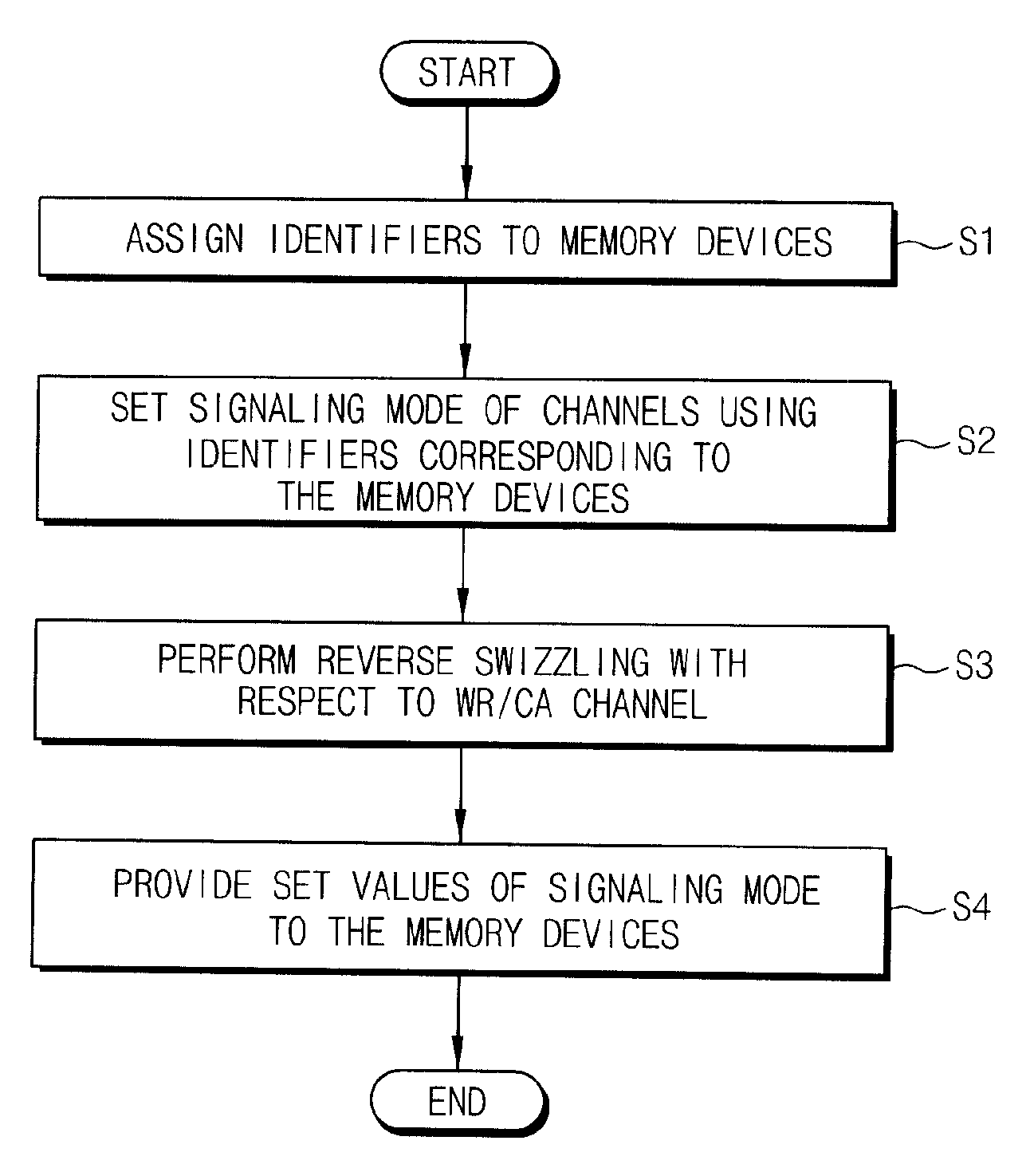
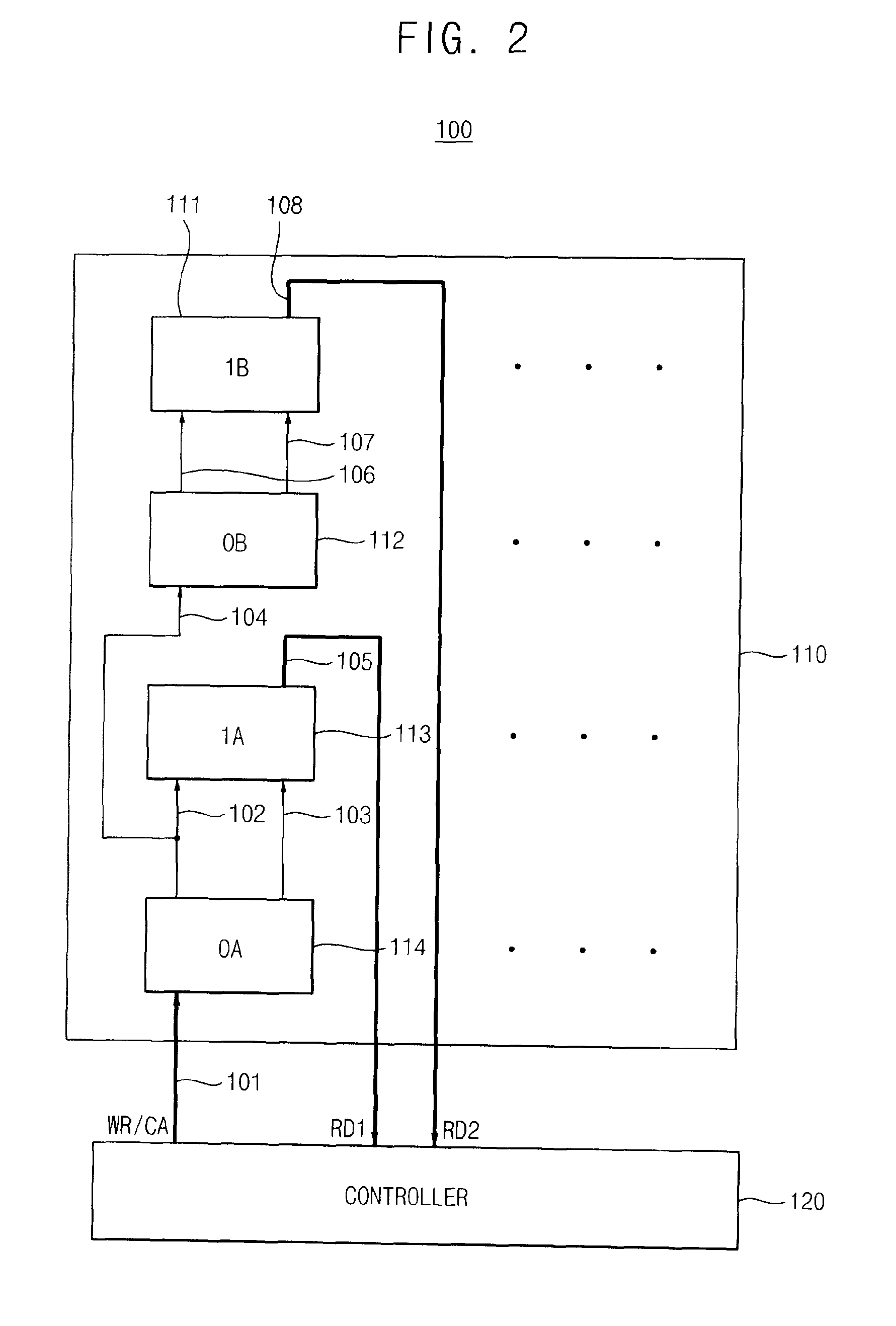
[0122]FIG. 12 is a block diagram illustrating a memory system according to the present invention.

[0123]Referring to FIG. 12, the memory system 800 includes a memory module 810 and a memory controller 820.

[0124]The memory module 810 includes a first semiconductor memory device (0A) 814, a second semiconductor memory device (1A) 813, a third semiconductor memory device (0B) 812 and a fourth semiconductor memory device (1B) 811. The memory controller 820 sets a signaling mode based on stack position information of each of the semiconductor memory devices 811, 812, 813 and 814. In FIG. 12, a bus drawn with a thick line represents a bus in which signaling is performed in a differential signaling mode, and a bus drawn with a thin line represents a bus in which signaling is performed in a single-ended signaling mode.

[0125]The first semiconductor memory device (0A) 814 receives a first packet WR / CA in the differential signaling mode through a first port (not shown) from the memory controlle...

tenth example embodiment

[0130]FIG. 13 is a block diagram illustrating a memory system 900 according to the present invention.

[0131]Referring to FIG. 13, the memory system 900 includes a memory module 910 and a memory controller 920.

[0132]The memory module 910 includes a first semiconductor memory device (0A) 914, a second semiconductor memory device (1A) 913, a third semiconductor memory device (0B) 912 and a fourth semiconductor memory device (1B) 911. The memory controller 920 sets a signaling mode based on stack position information of each of the semiconductor memory devices 911, 912, 913 and 914. In FIG. 13, a bus drawn with a thick line represents a bus in which signaling is performed in a differential signaling mode, and a bus drawn with a thin line represents a bus in which signaling is performed in a single-ended signaling mode.

[0133]The first semiconductor memory device (0A) 914 receives a first packet WR / CA in the differential signaling mode through a first port (not shown) from the memory contr...


PUM


Abstract

A memory system selectively sets signaling modes based on stack position information. The memory system includes a memory module having at least one semiconductor memory device and a memory controller configured to set a signaling mode based on stack position information of each of the semiconductor memory devices. A signaling between the memory controller and each of the semiconductor memory devices is performed in a differential signaling mode, and a signaling among the semiconductor memory devices is performed in a single-ended signaling mode. Accordingly, the memory system has reduced power consumption.

Description

CROSS-REFERENCE TO RELATED APPLICATIONS[0001]This application is a continuation-in-part of U.S. patent application Ser. No. 11 / 451,802, filed on Jun. 13, 2006, now pending, which is related to U.S. Provisional Patent Application Ser. No. 60 / 716,587, filed on Sep. 13, 2005, and which claims the benefit of priority under 35 USC §119 to Korean Patent Application No. 10-2005-0084813, filed on Sep. 12, 2005 in the Korean Intellectual Property Office (KIPO), and Korean Patent Application No. 10-2005-0087212, filed on Sep. 20, 2005 in the KIPO, the entire contents of all of the above applications being incorporated herein in their entirety by reference. This application also claims priority under 35 USC §119 to Korean Patent Application No. 10-2007-0001532, filed on Jan. 5, 2007 in the KIPO, the entire contents of which are incorporated herein in their entirety by reference.BACKGROUND OF THE INVENTION[0002]1. Field of the Invention[0003]The present invention relates to a memory system, and...

Claims


Application Information

Patent Timeline
Patent Type & Authority Patents(United States)
IPC IPC(8): G06F12/00G06F13/28G06F13/00
CPCG11C7/1075
Inventor CHUNG, HOE-JULEE, JUNG-BAECHOI, JOO-SUN
Owner SAMSUNG ELECTRONICS CO LTD
Why Eureka
Try Eureka