
Layout method of semiconductor circuit, program and design support system

a technology of semiconductor circuit and support system, applied in the direction of cad circuit design, program control, instruments, etc., can solve the problems of layout, loss of layout, and insufficient conventional technology in terms of optimizing the circuit,

Inactive Publication Date: 2011-04-26
SOCIONEXT INC
View PDF9 Cites 11 Cited by
  • Summary
  • Abstract
  • Description
  • Claims
  • Application Information

AI Technical Summary

Benefits of technology

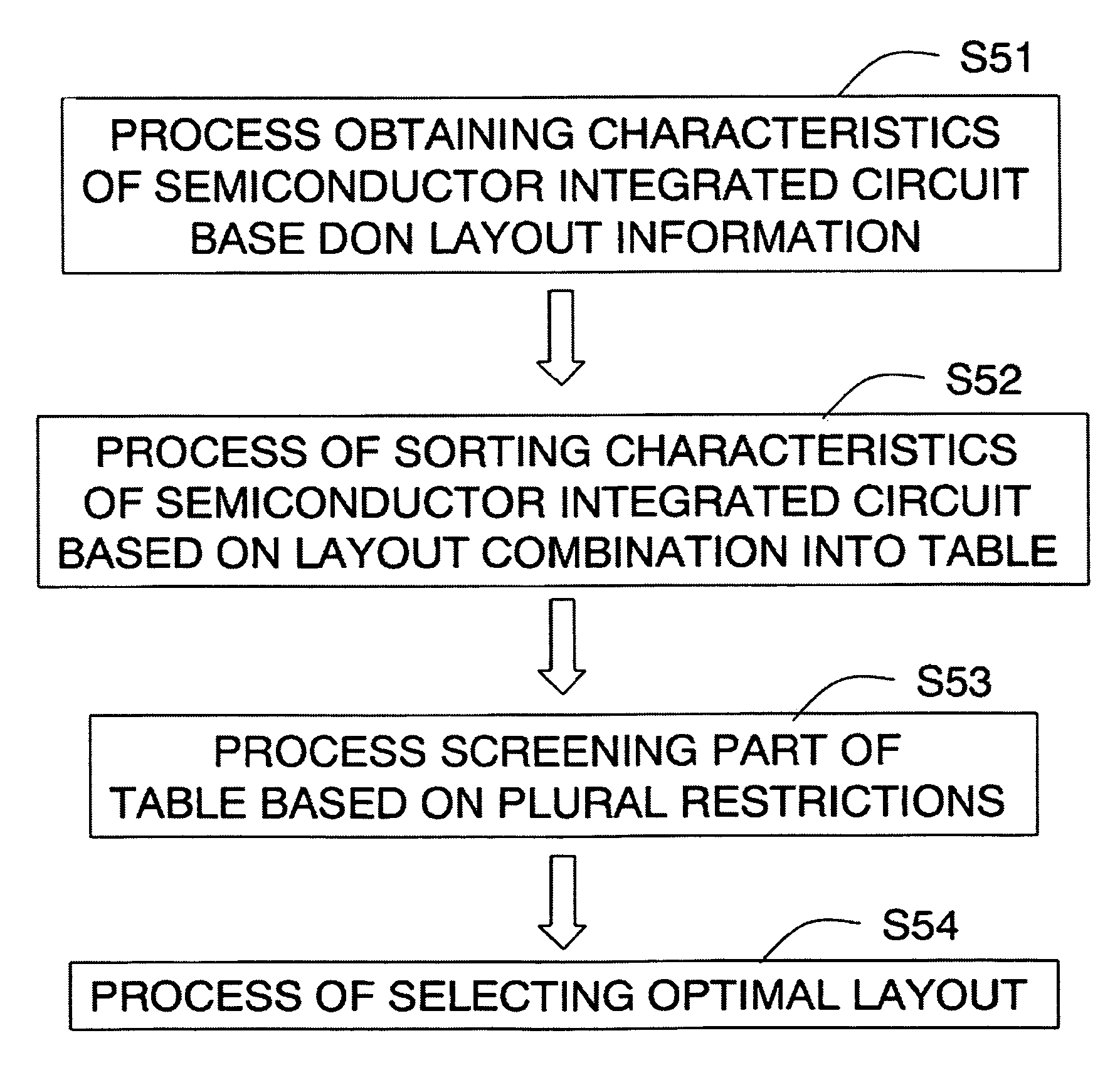
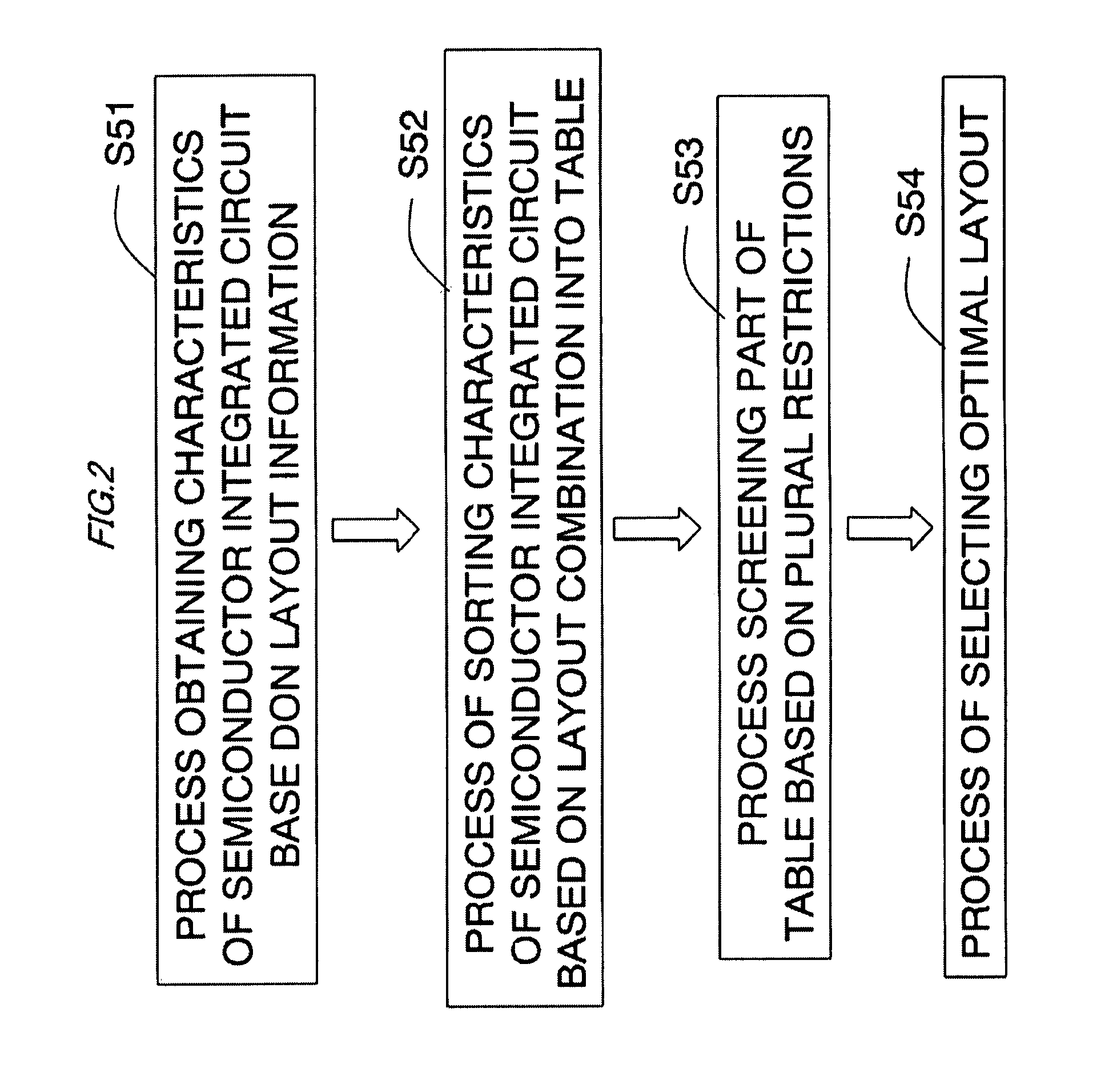
The patent describes a method for designing a semiconductor circuit by using information about the transistors in the circuit. This information is used to create a formula that can predict the performance of the circuit based on its layout. The method involves calculating multiple characteristic values based on the formula, selecting the best ones based on certain restrictions, and ultimately getting the final layout and transistor information. The technical effect of this method is to improve the accuracy and efficiency of semiconductor circuit design.

Problems solved by technology

A conventional technology is not, however, sufficient in terms of optimizing the circuit characteristics of a design target circuit as a whole including a multiplicity of devices and wirings due to a heavy load of calculation quantity.
The balance between the current driving force and the load in the actual circuit, which was taken into consideration when making the layout, might be lost.
Moreover, an analysis taking a plurality of circuit characteristics simultaneously into consideration, for example, a scheme of properly determining the gate length of each of the transistors of the circuit on the basis of a trade-off relationship between power consumption and circuit delay time, is not yet provided.

Method used


Image

  • Layout method of semiconductor circuit, program and design support system
  • Layout method of semiconductor circuit, program and design support system
  • Layout method of semiconductor circuit, program and design support system

Examples


embodiment

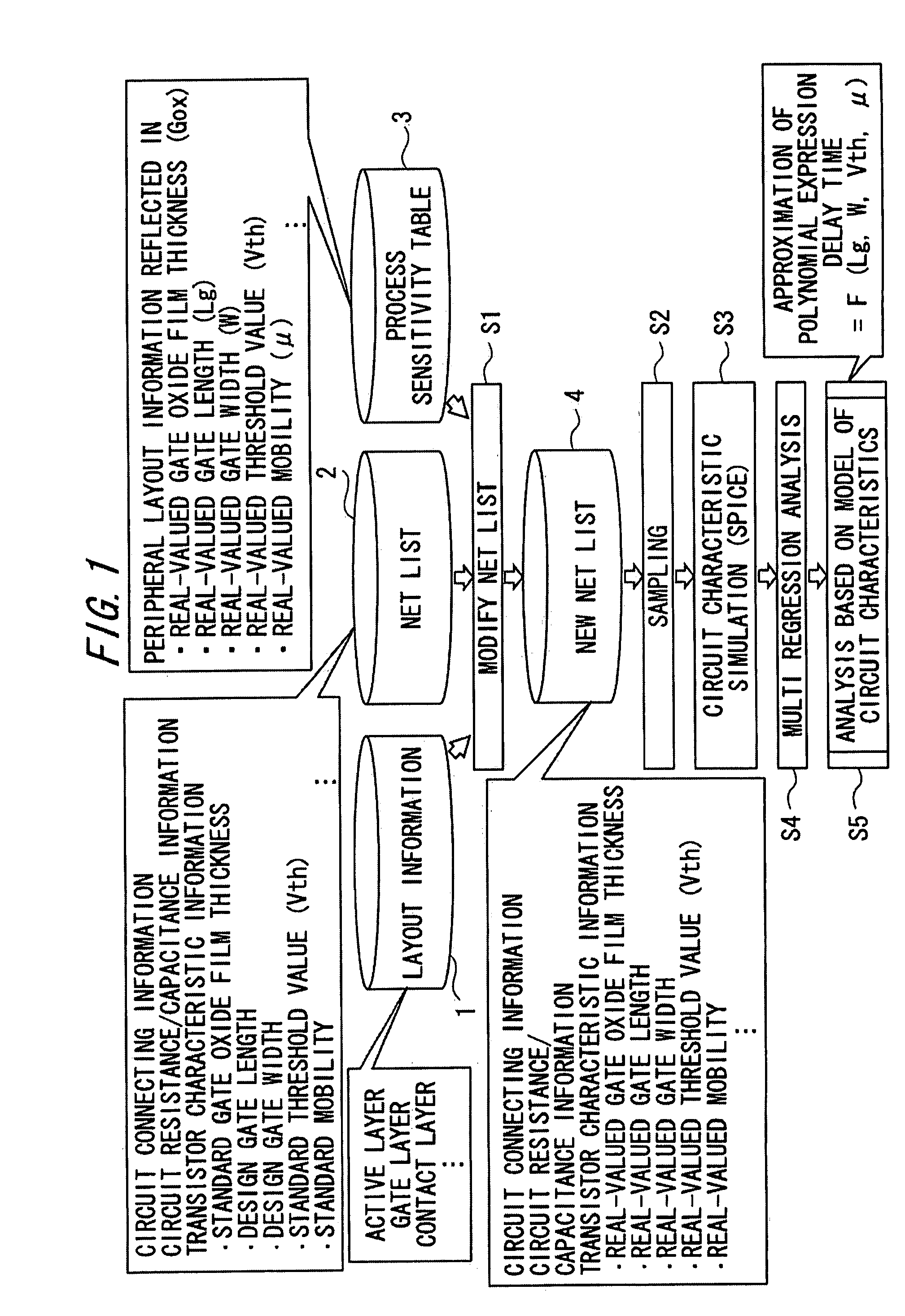
[0041]The design support tool according to an embodiment will be described with reference to the drawings in FIGS. 1 through 8. The design support tool is actualized as one function of a CAD (Computer Aided Design) system for designing an LSI (Large Scale Integration). The CAD system assumed herein is actualized on a general type of computer. The computer includes, e.g., a CPU, a memory, external storage units (such as a hard disk and a drive for a demountable portable recording medium), an interface with the external storage units, a communication interface, a display unit, and input / output units (for instance, a keyboard, a pointing device such as a mouse, etc).

[0042]The design support tool is actualized by a computer program executed on such a computer. The computer program is installed into the hard disk via the communication interface or the drive for the demountable portable recording medium. The CPU loads the installed computer program into the memory and then executes the pr...

first modified example

[0071]In the embodiment, the values of the terms in the polynomial expression are sequentially calculated, the contributions are added, and it is determined whether the circuit characteristics meet the limiting values or not. In such a process, among the combinations of the physical quantities (the combinations of the gate lengths Lg, the gate widths W, etc), which should be substituted into the variables of the polynomial expression, the combinations contrary to the design rule may previously be excluded.

[0072]Moreover, after calculating the contributions of the respective terms in the polynomial expression (e.g., after adding the contributions of the first term through the k−th term halfway in the polynomial expression ending with the N−th term), as to the contributions from the next term onward (the contributions of the (k+1)th term through the N−th term), the maximum value and the minimum value thereof are previously stored, and it may be determined based on the contribution of ...

second modified example

[0092]If the limiting values are strict, the combination of the physical quantities such as the gate length Lg, the gate width W, etc matching with the characteristics satisfying the limiting values, are not obtained. Whereas if the limiting values are not strict, it follows that the multiplicity of combinations are acquired. Such being the case, a desired number of combinations are designated, and the threshold may also be reset to obtain the combinations of the gate length Lg and the gate width W, of which the number is approximate to this desired number of combinations.

[0093]FIG. 10 shows a processing procedure of resetting the limiting value. In this process, the design support tool sets the maximum number of combinations when obtaining the combinations falling within the limiting values by the round-robin of the variable values (the gate length Lg, the gate width W, etc) of each transistor (S100). This setting may also be, for example, done in such a way that the user predeterm...


PUM


Abstract

A method of a layout a semiconductor circuit has obtaining transistor characteristic information on the basis of layout information about regions formed with transistors, obtaining a polynomial expression representing a relationship between characteristic values of a circuit including of the transistors and the transistor characteristic information, calculating a plurality of characteristic values corresponding to plural sets of transistor characteristic information by use of the polynomial expression, selecting part of the plurality of characteristic values on the basis of a restriction about the characteristic values, the layout information or the transistor characteristic information; and obtaining the transistor characteristic information or the layout information corresponding to the selected characteristic values.

Description

BACKGROUND OF THE INVENTION[0001]The present invention relates generally to a design of a semiconductor circuit, and more particularly to a technology of designing the semiconductor circuit, especially designing a circuit layout.[0002]As micronization of LSI has advanced over the recent years, circuit characteristics have been greatly affected by accuracy of physical quantities of a shape of layout pattern, arranging positions, etc of circuit devices(circuit elements) or by variations in these physical quantities in a manufacturing process. Further, such a method was also proposed that the circuit characteristics are optimized by taking the affection thereof into prediction of the circuit characteristics.[0003]A conventional technology is not, however, sufficient in terms of optimizing the circuit characteristics of a design target circuit as a whole including a multiplicity of devices and wirings due to a heavy load of calculation quantity. For example, the circuit design arranges ...

Claims


Application Information

Patent Timeline
Patent Type & Authority Patents(United States)
IPC IPC(8): G06F17/50
CPCG06F17/5068G06F17/5045G06F30/39G06F30/30G06F30/398
Inventor ARIMOTO, HIROSHI
Owner SOCIONEXT INC
Learn More