Semiconductor device, semiconductor device design method, semiconductor device design method recording medium, and semiconductor device design support system

a semiconductor device and design method technology, applied in computer aided design, program control, instruments, etc., can solve the problems of gate oxide film damage, gate oxide film pressure resistance significantly reduced, and change in transistor characteristics, so as to prevent antenna damage

Inactive Publication Date: 2006-09-26
PANASONIC CORP
View PDF24 Cites 10 Cited by
  • Summary
  • Abstract
  • Description
  • Claims
  • Application Information

AI Technical Summary

Benefits of technology

[0033]It is therefore an object of the invention to provide a semiconductor device, a semiconductor device design method, a semiconductor device design method recording medium, and a semiconductor device design support system capable of preventing antenna damage caused by an antenna effect occurring in a plasma step at the metal wiring formation time in a semiconductor process.

Problems solved by technology

The current causes such trouble of destruction of the gate oxide film, change in the transistor characteristics because of film quality change of the gate oxide film, or degradation of the hot carrier life.
First, the gate oxide film itself of a transistor becomes thin and pressure resistance of the gate oxide film considerably lowers as compared with the conventional process. There is an estimation that as the film is furthermore thinned, the antenna damage is remedied because the tunnel current in the gate oxide film grows. However, it is said that antenna rule proceeds toward the worse until at least the gate oxide film thickness of about 5 nm generally used with CMOS according to 0.25-μm design rule.
Second, the minimum gate width reduces with micro-miniaturization of process, but the wiring length is not much shortened although micro-miniaturization of process develops, because the signal wiring length does not lessen if the chip size set considering yield, etc., is micro-miniaturized to about 10 mm square.
Third, although damage caused by plasma entering from a side wall of wiring at the over-etching in a dry etching step of wiring is the main factor of the antenna damage, if the wiring width is thinned, the wiring film thickness cannot be so thinned for the purposes of providing resistance to electro-migration of wiring and suppressing the resistance value.
Fourthly, as the wiring pattern becomes fine, the plasma density at the etching time also tends to rise.
Therefore, to use such metal wiring running on one side of the chip of LSI having a chip size of 10 mm square as described above, the antenna rule is applied and the metal wiring becomes antenna wiring that can cause antenna damage.
However, this does not mean that whenever such an antenna ratio is applied, antenna damage occurs.
This means that if an aluminum pattern with the gate oxide film connecting to long aluminum wiring, not connected to the diffusion layer exists, an antenna rule error occurs.
Layout design considering the antenna rule is not yet general and effective countermeasures against antenna damage are not established as things stand now.
However, if diodes are embedded on mask operation all in wiring that can cause an antenna error, a wiring load problem arises; a load capacitance problem hardly occurs if a contact of the minimum size is added or so.
First, throughout all the countermeasures, an additional correction to an antenna error is required and when an attempt is made to use a CAD tool for automation, a clear and effective procedure does not exist. That is, an antenna rule error is frequently found at a one-chip wiring layout stage close to the end of design and the current automatic placement wiring tool of CAD does not provide a function for avoiding an antenna rule error. Therefore, with the current state of the art, the designer manually takes such measures of adding an antenna protection diode to a device for which an error is found at the stage where a mask order is about to be given. Such a relapse in the design stage and occurrence of manual work become the largest problem in design automation.
This means that to provide a wiring route passing through the diffusion layer at an intermediate point of metal wiring, a large resistance value is added as compared with the metal wiring owing to the diffusion layer, worsening the circuit operation speed.
A common problem to the first and second countermeasures is to place limitations on a design style.
For example, at completion of a chip at the block level, if the blocks are placed and a mask order is given from the ground and diffusion is started on one hand and layout design is furthermore advanced and an antenna rule error is found in the later layout design using aluminum wiring on an upper layer on the other hand, the error cannot be handled by changing the design of the lower layer.
However, if the error occurrence frequency increases, wiring corrections as countermeasures against the antenna rule errors are made to the device with wiring well laid out, largely changing the congestion degree of the upper layer aluminum wiring and the wiring pattern.
Then, when the wiring is again executed, it cannot be fitted as the same area as before the antenna rule error corrections are made is held, or the wiring congestion degree and the wiring length are changed, thus new trouble of occurrence of a timing error on logical circuit design not previously occurring is caused.
In the recent LSI design, signals whose wiring delay is to be suppressed have been wired at gentle pitches with thick metal film wiring of an upper layer as much as possible; an increase in the congestion degree of the upper layer wiring is undesirable for speed performance.

Method used


Image

  • Semiconductor device, semiconductor device design method, semiconductor device design method recording medium, and semiconductor device design support system
  • Semiconductor device, semiconductor device design method, semiconductor device design method recording medium, and semiconductor device design support system
  • Semiconductor device, semiconductor device design method, semiconductor device design method recording medium, and semiconductor device design support system

Examples


first embodiment

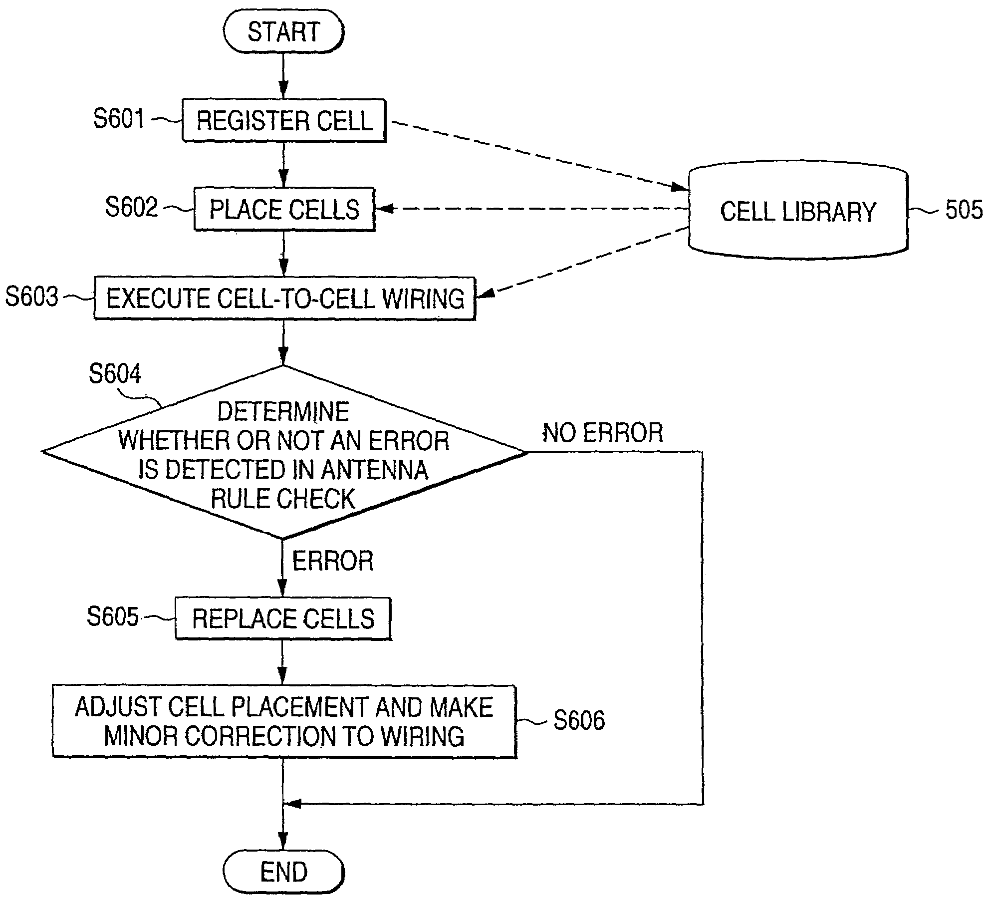
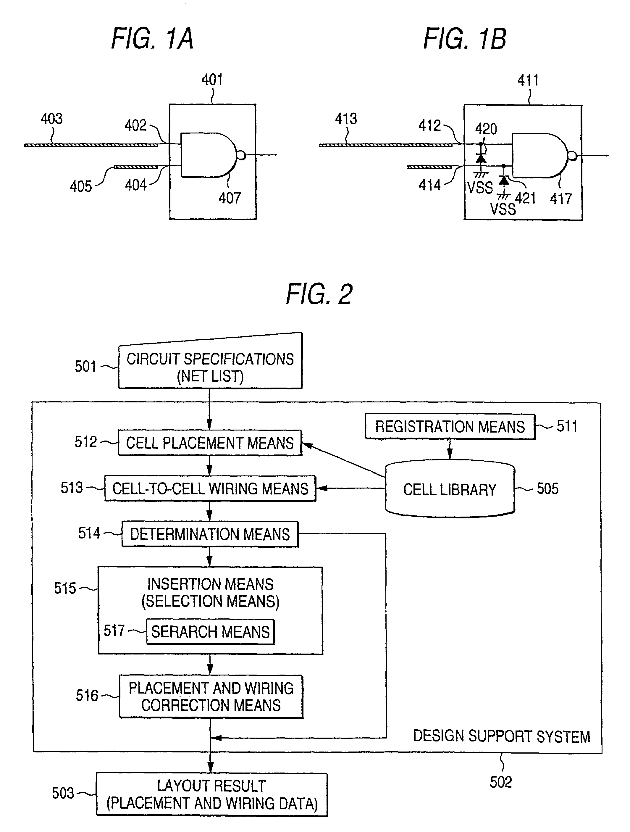
[0073]Next, a semiconductor device, a semiconductor device design support system, and a semiconductor device design method according to a first embodiment will be discussed with reference to FIGS. 1 to 3. FIGS. 1A and 2B are schematic diagrams to conceptually describe a layout of the semiconductor device of the first embodiment. FIG. 2 is a block diagram of the semiconductor device design support system of the first embodiment. FIG. 3 is a flowchart to describe the semiconductor device design method of the first embodiment.

[0074]The embodiment is characterized by the fact that first-kind cells each comprising an n+ diffusion layer-P well type protection diode (or a p+ diffusion layer-N well type antenna protection diode; for the structures of the diodes, see FIGS. 17A and 16B) connected to an input pin for preventing antenna damage or an antenna rule error from occurring and second-kind cells each not containing the protection diode and having the same logic as and the same drive ca...

third embodiment

[0091]Next, a semiconductor device, a semiconductor device design support system, and a semiconductor device design method according to a third embodiment will be discussed with reference to FIG. 15. FIG. 15 is a schematic diagram to conceptually describe a layout of the semiconductor device of the fourth embodiment.

[0092]In FIG. 15, parts (a) and (b) are schematic diagrams to show a state in which an unused input pin of an inverter 2041 is connected to a power supply trunk and potential is fixed. The part (a) is a plan schematic diagram viewed from above the semiconductor device and the part (b) is a sectional schematic diagram taken on line A–A′ in the part (a). In FIG. 15, the unused input pin of the inverter 2041 is connected via first metal wiring 2015 to a second metal power supply trunk 2021 (2022) and potential is fixed. The second metal power supply trunk 2021 (2022) is connected to a third metal power supply trunk 2031. The second metal power supply trunk 2021 indicates wi...

fourth embodiment

[0095]Next, a semiconductor device, a semiconductor device design support system, and a semiconductor device design method according to a fourth embodiment will be discussed with reference to FIGS. 6A to 6D. FIGS. 6A to 6D are schematic diagrams to conceptually describe a layout of the semiconductor device of the fifth embodiment.

[0096]The embodiment is characterized by the fact that when it is assumed that the ratio between the area of a wiring conductor conducting to a gate electrode and the area of the gate electrode is an antenna ratio, each wiring conductor conducting to a gate electrode in each wiring layer is limited to the area or wiring length as an antenna ratio of less than a half the allowed antenna ratio in the semiconductor device and is divided into at least three parts for wiring.

[0097]The semiconductor device of the embodiment will be discussed with reference to the schematic diagrams of FIGS. 6A to 6D. FIG. 6A schematically shows a wiring layout of metal wiring 902...


PUM


Abstract

Repeater cells each comprising a buffer or an inverter and an n+ diffusion layer-P well type protection diode or a p+ diffusion layer-N well type antenna protection diode connected to an input pin of the buffer or the inverter for preventing antenna damage or an antenna rule error from occurring are previously registered by registration means 511 as the cells to be registered in a cell library 505. Whether or not a wiring conductor conducting to a gate electrode becomes an antenna ratio exceeding an allowed antenna ratio in the semiconductor device is determined by determination means 514 and if the wiring conductor exceeds the allowable antenna ratio, one or more repeater cells are inserted into any point of the wiring conductor by selection means 515.

Description

BACKGROUND OF THE INVENTION[0001]This invention relates to a semiconductor device, a semiconductor device design method, a recording medium recording a program for executing the semiconductor device design method, and a semiconductor device design support system and in particular to a semiconductor device, a semiconductor device design method, a semiconductor device design method recording medium, and a semiconductor device design support system capable of preventing antenna damage caused by an antenna effect occurring in a plasma step at the metal wiring formation time in a semiconductor process.[0002]In recent semiconductor process wiring steps, various plasma techniques have been used. The representative plasma techniques include dry etching at the wiring layer patterning, plasma TEOS film deposition of wiring layer insulating film in a multi-layered wiring step, and the like, for example, which will be hereinafter referred to as plasma steps.[0003]For example, when plasma etchin...

Claims


Application Information

Patent Timeline
Patent Type & Authority Patents(United States)
IPC IPC(8): G06F17/50H01L21/302H01L21/3065H01L21/336H01L21/82H01L23/485H01L27/00H01L27/02H01L27/118H01L29/78
CPCG06F17/5072H01L24/02H01L27/0255H01L27/118H01L27/11807G06F17/5077H01L2924/01075H01L2924/01002H01L2924/01004H01L2924/01005H01L2924/01006H01L2924/01013H01L2924/01015H01L2924/01033H01L2924/01079H01L2924/01082H01L2924/30105H01L2924/01019G06F30/394G06F30/392
Inventor ISHIKURA, SATOSHI
Owner PANASONIC CORP
Why Eureka
Try Eureka