Method and apparatus for wafer level burn-in

a technology of burnin and wafers, applied in the direction of fault location by increasing the damage at fault, semiconductor/solid-state device testing/measurement, instruments, etc., can solve the problems of defective products flowing into the market, insufficient temperature load screening, and serious damage, and achieve high reliability

Inactive Publication Date: 2011-05-10
SOCIONEXT INC
View PDF18 Cites 27 Cited by
  • Summary
  • Abstract
  • Description
  • Claims
  • Application Information

AI Technical Summary

Benefits of technology

[0014]The invention is made to solve the aforementioned problems, and an object of the invention is to provide a wafer level burn-in method and a wafer level burn-in apparatus with high reliability, which do not depend on the distribution of conforming products of devices formed on a wafer and the power consumption of the devices, and in which variation in in-plane temperature of the wafer due to the generation of heat at the time of applying an electric load is reduced to prevent probes from being consumed and burnt.

Problems solved by technology

When the temperature of a part of the wafer increases due to a decrease in in-plane uniformity, the probe for applying an electric load to the water may be extremely consumed or burnt out to result in serious damage.
When the temperature of a part of the wafer decreases, it is insufficient to perform screening by the temperature load.
Accordingly, defective products may flow into the market.

Method used


Image

  • Method and apparatus for wafer level burn-in
  • Method and apparatus for wafer level burn-in
  • Method and apparatus for wafer level burn-in

Examples


embodiment 1

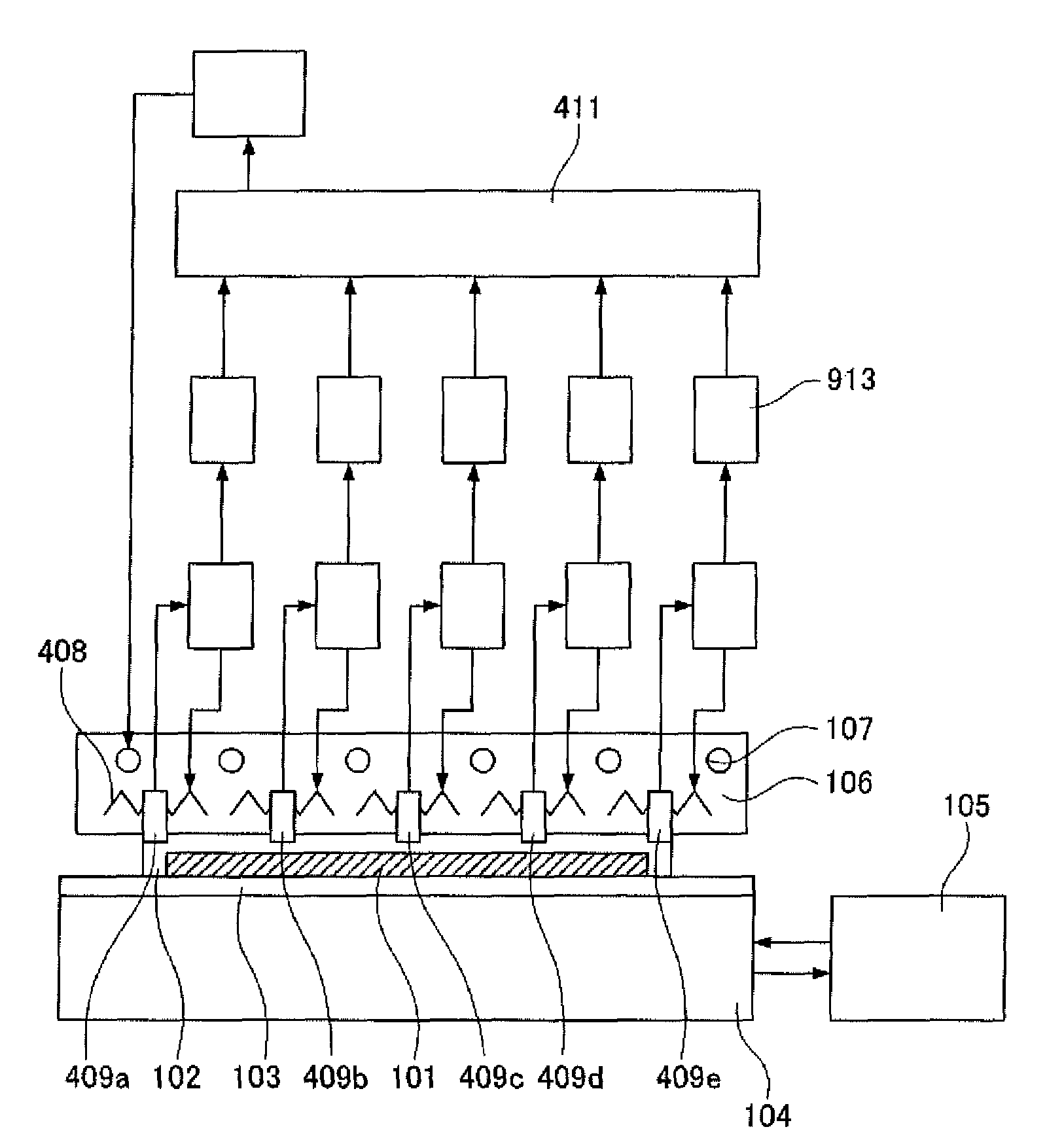
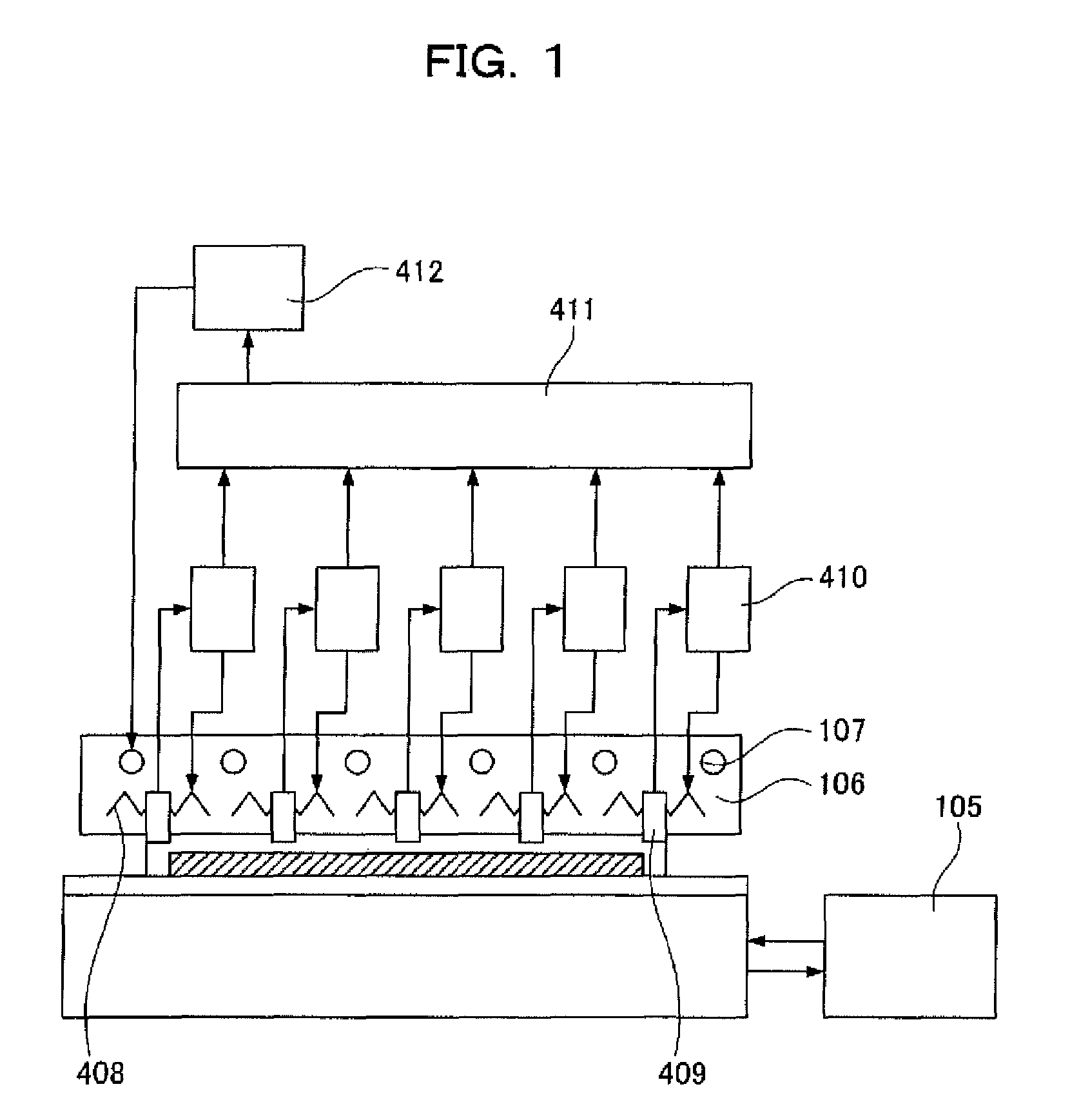
[0052]A wafer level burn-in apparatus and a wafer level burn-in method according to Embodiment 1 will be described with reference to FIGS. 1, 2, 3, and 4.

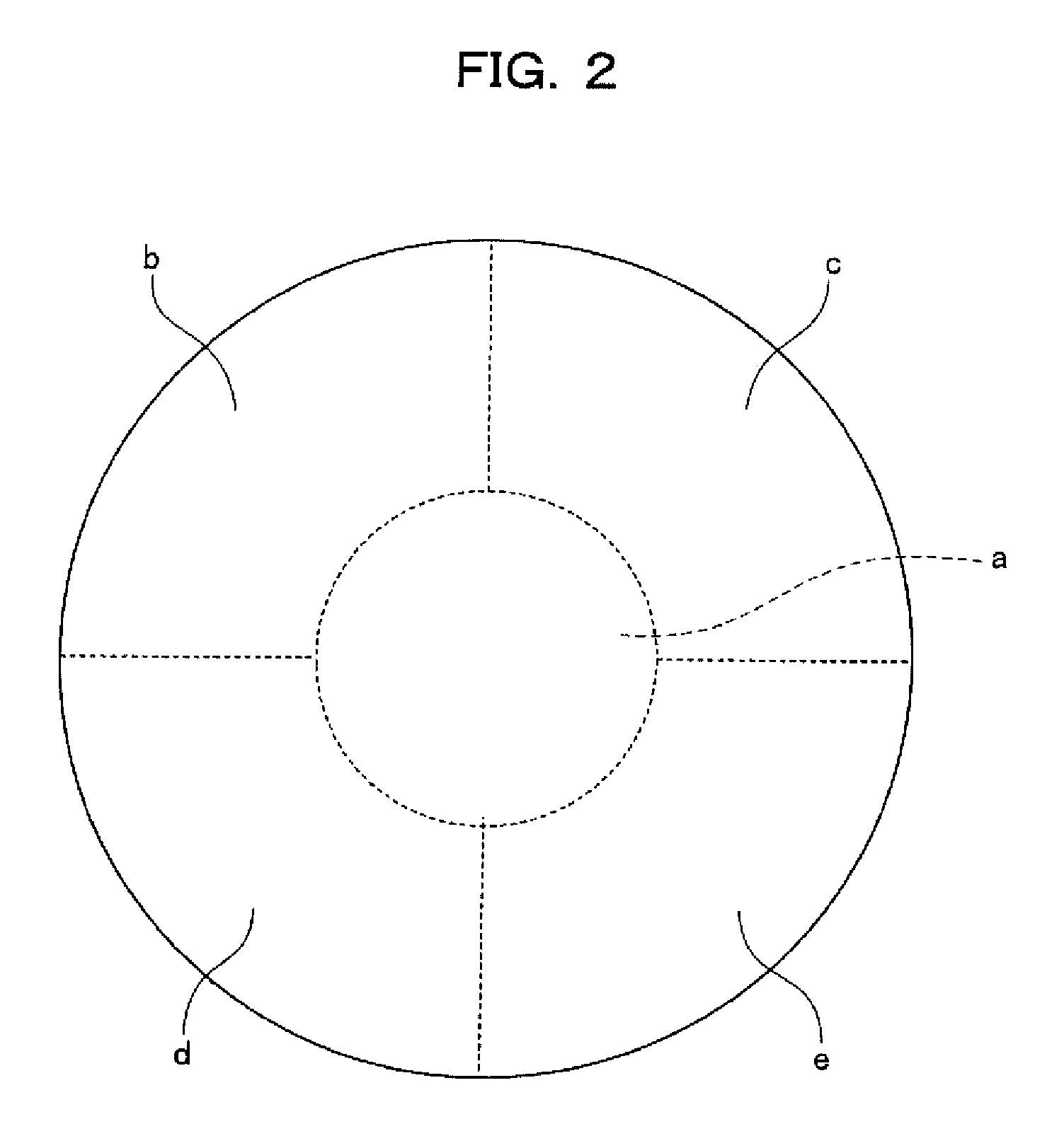
[0053]FIG. 1 is a schematic diagram illustrating the wafer level burn-in apparatus according to Embodiment 1. FIG. 2 is a diagram illustrating area division of a temperature regulation plate according to Embodiment 1 of the invention. FIG. 3 is a schematic diagram illustrating a temperature control system for the temperature regulation plate according to Embodiment 1 of the invention. FIG. 4 is a diagram illustrating temperature control at the time of wafer level burn-in according to Embodiment 1 of the invention.

[0054]In Embodiment 1 shown in FIG. 1, as compared with the configuration of a device shown in FIG. 9, a temperature regulation plate 106 is divided into five areas of a central area a and its peripheral areas b to e as shown in FIG. 2, one heater 108, one temperature sensor 109, and one temperature regulator 110 for each ...

embodiment 2

[0060]A wafer level burn-in apparatus and a wafer level burn-in method according to Embodiment 2 will be described with reference to FIGS. 1, 2, 3, and 5.

[0061]FIG. 5 is a diagram illustrating temperature control at the time of wafer level burn-in according to Embodiment 2 of the invention.

[0062]In Embodiment 2 of the invention, the same device configuration as Embodiment 1 shown in FIGS. 1, 2, and 3 is used.

[0063]In the wafer level burn-in according to Embodiment 2, heating control is performed for each area so that all the predetermined values of temperature sensors 409a to 409e are 125° C. The flow rate of refrigerant is controlled by selecting the median value among the values measured by the temperature sensors 409a to 409e and performing the cooling operation with respect to the predetermined value of 125° C.

[0064]FIG. 5 is a graph illustrating the transition of the areas in which the temperatures selected as a control target of the refrigerant flow rate are measured, a tempor...

embodiment 3

[0067]A wafer level burn-in apparatus and a wafer level burn-in method according to Embodiment 3 will be described with reference to FIGS. 1, 2, 3, and 6.

[0068]FIG. 6 is a diagram illustrating temperature control at the time of wafer level burn-in according to Embodiment 3 of the invention.

[0069]In Embodiment 3 of the invention, the same device configuration as Embodiment 1 shown in FIGS. 1, 2, and 3 is used.

[0070]In the wafer level burn-in according to Embodiment 3, the heating control is performed for each area so that all predetermined values of temperature sensors 409a to 409e are 125° C. The flow rate of refrigerant is controlled by selecting the value closest to the average value of values measured by the temperature sensors 409a to 409e among the values or selecting the higher value where there are two candidate values, and performing cooling operation with respect to the predetermined value of 125° C.

[0071]FIG. 6 is a graph illustrating the transition of the areas in which t...


PUM


Abstract

A temperature regulation plate 106 is divided into at least two areas, a heater 408 for applying a temperature load in correspondence with such areas and its control system are divided and controlled independently to set temperatures, and a cooling source is controlled by comparing the measurements from temperature sensors 409 arranged in respective areas for controlling the heater 408 and switching the measurement for calculating the control output sequentially thus reducing variation in in-plane temperature of a wafer due to heating when an electric load is applied. Since consumption and burning of a probe are prevented, highly reliable wafer level burn-in method and apparatus can be provided.

Description

TECHNICAL FIELD[0001]The present invention relates to a wafer level burn-in method and a wafer level burn-in apparatus to perform screening by applying an electric load and a temperature load to a semiconductor wafer.BACKGROUND ART[0002]Conventionally, a screening test device generally called as a burn-in apparatus performs screening of defective products in such a manner that, after packaging IC chips obtained by dividing a semiconductor wafer, a current applying test of the packaged IC chips is performed in a thermal atmosphere at a predetermined temperature (e.g., 125° C.), and thus latent defects are exposed.[0003]Since such a conventional device needs a large constant-temperature device and has a large calorific value, the device needs to operate in a room separated from other production lines. Accordingly, it is desired to perform a burn-in test in a wafer level before becoming a chip because of: troubles such as transport of a wafer, attachment to and detachment from a device...

Claims


Application Information

Patent Timeline
Patent Type & Authority Patents(United States)
IPC IPC(8): G01R31/00
CPCG01R31/2874H01L21/67103H01L21/67288H01L21/67248H01L21/67242H01L22/00
Inventor SEGAWA, TERUTSUGUSANADA, MINORU
Owner SOCIONEXT INC
Why Eureka
Try Eureka