Circuit board structure

a technology of circuit board and structure, applied in the direction of resistive material coating, gas-filled discharge tube application, non-metallic protective coating, etc., can solve the problems of reducing the power quality and capability of the circuit, the impedance between lines, and the disadvantage of fabricating circuits of fine lines, so as to reduce the overall thickness, enhance fluidity, and high insulation

Active Publication Date: 2011-05-24
UNIMICRON TECH CORP
View PDF22 Cites 12 Cited by
  • Summary
  • Abstract
  • Description
  • Claims
  • Application Information

AI Technical Summary

Benefits of technology

[0011]In view of the disadvantages of the prior art mentioned above, it is a primary objective of the present invention to provide a circuit board structure and a fabrication method of the same, which are capable of avoiding drawbacks of inefficient insulation of lines caused by poor fluidity and filling of a solder mask.
[0012]It is another objective of the present invention to provide a circuit board structure and a fabrication method of the same, which are capable of enhancing insulating property of the solder mask.
[0013]It is a further objective of the present invention to provide a circuit board structure and a fabrication method of the same, which are capable of decreasing migration of metal atoms in the solder mask.

Problems solved by technology

The outcome is definitely a disadvantageous situation for fabricating circuit of fine lines.
Besides, the solder mask 12 with macroparticles has relatively poor insulation and a relatively high dielectric constant, thus migration of metal atoms of the circuit layer 11 in the solder mask 12 is likely to happen, and consequently impedance between lines will not fit in with product specification, and then electric signal interference between lines happens; in a worse scenario of migration of metal atoms, the solder mask 12 will produce metal hyphae, in such situation, when the circuit layer 11 is electrified, terminals of the metal hyphae tend to discharge electricity, consequently electricity quality and capability of the circuit are greatly diminished; it is obviously that the pitches between lines should be spacious enough to prevent migration of metal atoms from happening, therefore the demand for applying fine circuit lines cannot be reached.

Method used


Image

  • Circuit board structure
  • Circuit board structure
  • Circuit board structure

Examples


first embodiment

[0029]Please refer to FIGS. 2A through 2I, which are cross-sectional views illustrating the first embodiment of a fabrication method of a circuit board structure according to the present invention.

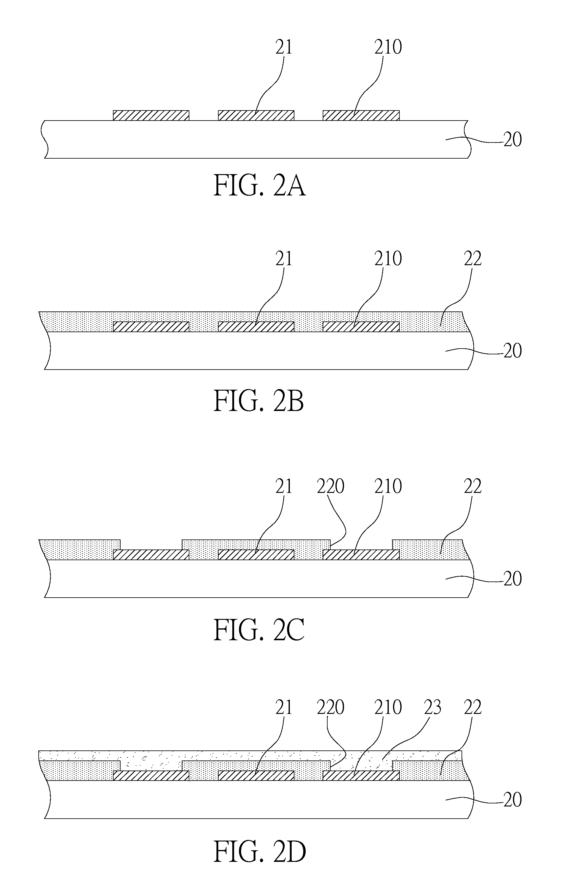
[0030]As shown in FIG. 2A, the first embodiment of a fabrication method of a circuit board structure according to the present invention comprises providing a carrier board 20 with at least one surface formed with a circuit layer 21 having a plurality of electrically connecting pads 210.

[0031]As shown in FIG. 2B, forming a first solder mask 22 on top of the carrier board 20 and the circuit layer 21 by means of printing, spin coating, or laminating, such that the first solder mask 22 is higher than the top of the circuit layer 21. The solder mask 22 is made of a high-insulation photosensitive material characterized by presence or absence of impurities, such as microparticles.

[0032]As shown in FIG. 2C, forming a plurality of first openings 220 in the first solder mask 22 by a patterning proce...

second embodiment

[0042]Please refer to FIGS. 3A through 3H, which are cross-sectional views illustrating the second embodiment of a fabrication method of a circuit board structure of the present invention.

[0043]As shown in FIG. 3A, the second embodiment of a fabrication method of a circuit board structure of the present invention comprises providing a carrier board 20 (which is the same as the carrier board 20 in the first embodiment) with at least one surface formed with a circuit layer 21 having a plurality of electrically connecting pads 210.

[0044]As shown in FIG. 3B, forming a first solder mask 22 on top of the carrier board 20 and the circuit layer 21 such that the first solder mask 22 is higher than the top of the circuit layer 21. The first solder mask 22 is made of a high-insulation photosensitive material characterized by presence or absence of impurities, such as microparticles.

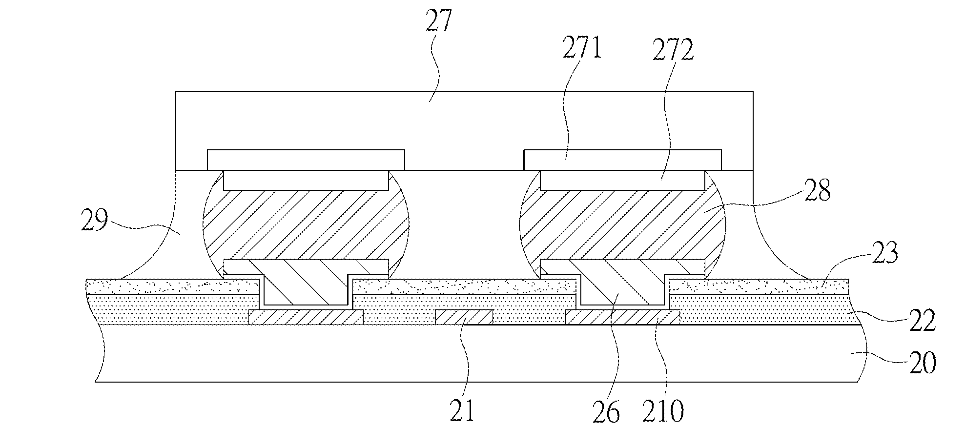
[0045]As shown in FIG. 3C, forming a second solder mask 23 on top of the first solder mask 22. The second solder ...


PUM

PropertyMeasurementUnit
dielectric constantsaaaaaaaaaa
thicknessesaaaaaaaaaa
thicknessaaaaaaaaaa

Abstract

A circuit board structure and a fabrication method of the same are disclosed according to the present invention. The circuit board structure includes: a carrier board with at least one surface formed with a circuit layer having electrically connecting pads; a first solder mask formed on the carrier board and the circuit layer and formed with first openings for exposing the electrically connecting pads; and a second solder mask formed on the first solder mask and formed with second openings for exposing the first openings and the electrically connecting pads. The first solder mask is made of a high-insulation photosensitive material characterized by presence or absence of impurities, such as microparticles, to have enhanced fluidity for being filled in the circuit layer, thereby preventing metal ions migration and subsequent metal hypha electricity discharge which might otherwise affect electrical performance, therefore the present invention is applicable to fine circuit fabrication.

Description

BACKGROUND OF THE INVENTION[0001]1. Field of the Invention[0002]The present invention generally relates to circuit board structures and fabrication methods of the same, and more specifically, to a circuit board structure with fine circuits and a fabrication method of the same.[0003]2. Description of Related Art[0004]Owing to the evolution of semiconductor package technology, different package models of semiconductor devices have been developed. A traditional method for fabricating semiconductor devices comprises the following steps: mounting a semiconductor element, e.g. an integrated circuit, on a package substrate or a leadframe; electrically connecting the semiconductor element to the package substrate or the leadframe and performing encapsulation with an encapsulant; wherein ball grid arrays (BGAs), such as PBGA, EBGA, FCBGA, and others, are advanced semiconductor package technologies applied. The features of these technologies are: mounting a semiconductor element on one side o...

Claims


Application Information

Patent Timeline
Patent Type & Authority Patents(United States)
IPC IPC(8): H05K1/02H05K3/00B32B3/10
CPCH01L2224/05018H05K3/0023H05K3/243H05K3/28H05K3/3473H05K3/4007H05K2201/0367H05K2201/09436H05K2201/09845H05K2203/054H05K2203/0577Y10T428/24273
Inventor SHIH, CHAO-WENZENG, ZHAO-CHONG
Owner UNIMICRON TECH CORP
Why Eureka
Try Eureka