Wiring structure in a semiconductor device

a wiring structure and semiconductor technology, applied in semiconductor devices, semiconductor/solid-state device details, electrical apparatus, etc., can solve the problems of corrosion inside the copper wiring, inability to pattern the copper wiring, and often inferior crystalline relative of the wiring layer, so as to avoid electrical insulation and avoid generation of voids.

Inactive Publication Date: 2005-08-30
RENESAS ELECTRONICS CORP
View PDF22 Cites 8 Cited by
  • Summary
  • Abstract
  • Description
  • Claims
  • Application Information

AI Technical Summary

Benefits of technology

[0050]In view of the above-mentioned problems in the conventional wiring structure, it is an object of the present invention to provide a copper wiring structure which is capable of avoiding generation of void caused by copper migration, and further avoiding electrical insulation between wiring layers.

Problems solved by technology

When a copper wiring is to be patterned, if a copper wiring is etched in the same manner as an aluminum wiring, copper is harmfully affected by etching gas and moisture, resulting in that corrosion occurs inside the copper wiring.
Accordingly, unlike an aluminum wiring, it is not suitable to pattern a copper wiring through the use of a photoresist mask and etching gas.
As a result, a wiring layer having a small width often has inferior crystalline relative to a wiring layer having a great width.
A thin copper film having been agglomerated is no longer able to be used as a material of which a copper wiring is composed.
This is because, if a copper film were agglomerated, the copper film would contain void, and resultingly, would have wiring defects such as breakage.
The above-mentioned dual-damascene multi-layered wiring structure is accompanied with a problem of void caused by the above-mentioned migration of copper.
However, the damascene wiring structure illustrated in FIGS. 4A and 4B is accompanied with a problem that it has to carry out complex photolithography and etching steps in order to form the projections 134, resulting in reduction in a fabrication yield.

Method used


Image

  • Wiring structure in a semiconductor device
  • Wiring structure in a semiconductor device
  • Wiring structure in a semiconductor device

Examples


first embodiment

[First Embodiment]

[0108]FIG. 5 is an upper plan view of a wiring structure 10 in accordance with the first embodiment of the present invention, and FIG. 6 is a perspective view of the wiring structure 10 illustrated in FIG. 5.

[0109]For instance, the wiring structure 10 can be applied to a semiconductor device as a part of a planar wiring pattern.

[0110]The wiring structure 10 is comprised of a first wiring layer 11, and a second wiring layer 12 electrically and physically connected to the first wiring layer 11. The first and second wiring layers 11 and 12 are formed in a common layer, and both composed of copper (Cu).

[0111]As illustrated in FIGS. 5 and 6, the first wiring layer 11 has a length L1, a width W1 and a height H1, and the second wiring layer 12 has a length L2, a width W2 and a height H2. The width W2 of the second wiring layer 12 is greater than the width W1 of the first wiring layer 11 (W2>W1)

[0112]A volume V1 of the first wiring layer 11 and a volume V2 of the second wi...

second embodiment

[Second Embodiment]

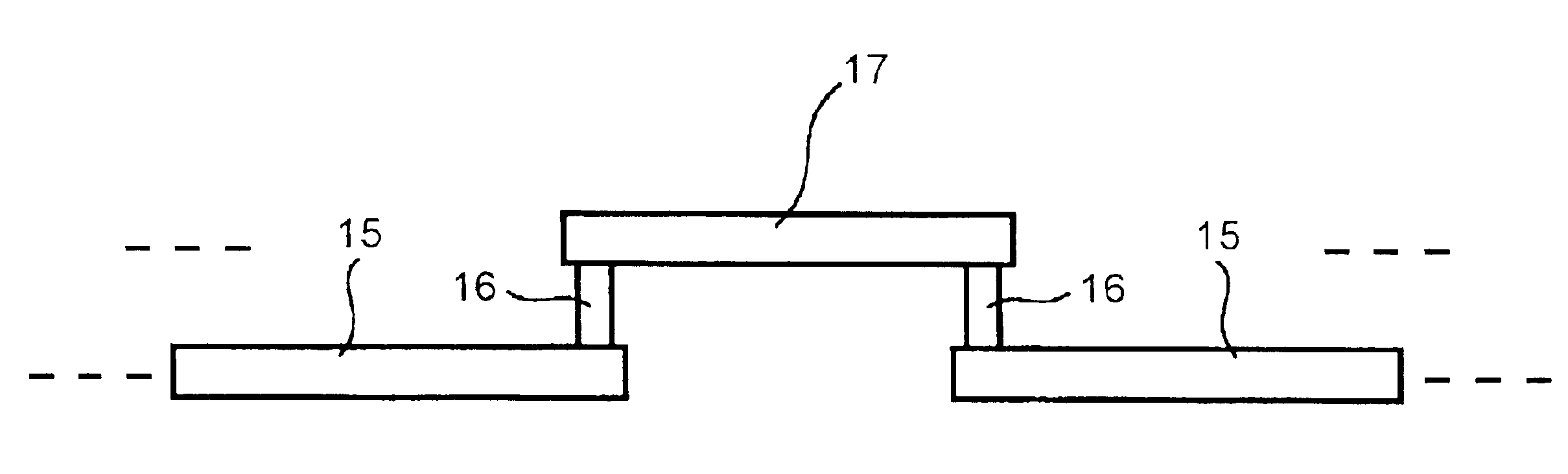
[0154]FIGS. 13A and 13B illustrate a wiring structure 20 in accordance with the second embodiment of the present invention.

[0155]FIG. 13A is a plan view of the wiring structure 20, and FIG. 13B is a cross-sectional view taken along the line 12B—12B in FIG. 13A.

[0156]The wiring structure 20 is applicable to a multi-layered wiring structure in a semiconductor device, for instance.

[0157]The wiring structure 20 in accordance with the second embodiment is comprised of a first lower wiring layer 21a, a second lower wiring layer 21b, an upper wiring layer 22 arranged above and across the first and second lower wiring layers 21a and 21b, a first via-conductor 23a electrically connecting the first lower wiring layer 21a and the upper wiring layer 22 to each other, and a second via-conductor 23b electrically connecting the second lower wiring layer 21b and the upper wiring layer 22 to each other.

[0158]The first and second lower wiring layers 21a and 21b, the upper wiring la...


PUM


Abstract

A wiring structure includes a first wiring having a first wiring width, and a second wiring formed in the same layer as a layer in which the first wiring is formed, and having a second wiring width greater than the first wiring width. The second wiring is electrically connected to the first wiring. Both of the first and second wirings are composed of copper or an alloy predominantly containing copper therein. The first and second wirings have the same thickness as each other. A ratio of an area of the second wiring to an area of the first wiring is N:1 where N is equal to or greater than 2,000 and equal to or smaller than 200,000,000 (2,000≦N≦200,000,000).

Description

BACKGROUND OF THE INVENTION[0001]1. Field of the Invention[0002]The invention relates to a wiring structure and a semiconductor device including the wiring structure, and more particularly to a dual-damascene wiring structure and a semiconductor device including the dual-damascene wiring structure.[0003]2. Description of the Related Art[0004]In a conventional semiconductor device, a metal wire has been usually composed of aluminum or aluminum alloy. This is because aluminum and aluminum alloy can be readily patterned through the use of a photoresist mask and etching gas, since aluminum and aluminum alloy have a low resistivity.[0005]In these days, with reduction in a size of a semiconductor device and increase in an operation rate of a semiconductor device, there is a need for a material of which a wiring is to be composed and which has a lower resistivity and a higher current density than aluminum and aluminum alloy. As a material meeting with such requirements, copper (Cu) draws m...

Claims


Application Information

Patent Timeline
Patent Type & Authority Patents(United States)
IPC IPC(8): H01L21/70H01L23/52H01L23/532H01L21/768H01L23/528H01L21/3205H01L23/522
CPCH01L21/76838H01L21/76877H01L23/528H01L23/53228H01L2924/0002H01L2924/00
Inventor MATSUBARA, YOSHIHISAOKADA, NORIO
Owner RENESAS ELECTRONICS CORP
Why Eureka
Try Eureka