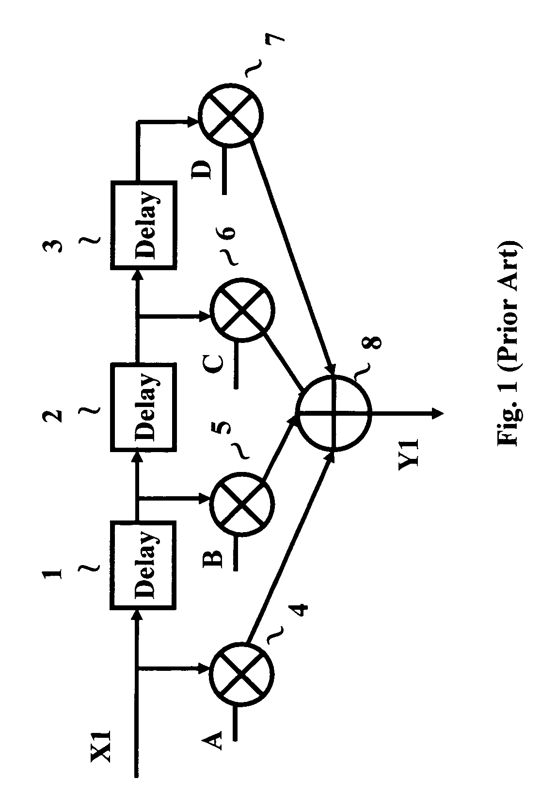
[0008]Accordingly, it is a primary object of the present invention to provide an analog FIR and IIR filter implementation that improves upon the speed of current implementations into the hundreds of gigahertz range with superior linearity to the implementations of the prior art.
[0009]The present invention achieves the above objectives and advantages by taking advantage of the properties of transmission lines. A transmission line provides a fixed impedance value over a wide range of frequencies with excellent linearity. This easily includes ranges up to and exceeding 100 GHz. In addition, the propagation delay of signals propagating down a transmission line can be precisely controlled only by the dimensions of the transmission line and the physical properties of the medium in which the transmission line is built. The inventor notes that these properties of the transmission line make it an ideal element for the delay stages of the FIR filter and are not subject to the linearity / bandwidth limitations of active delay stages.
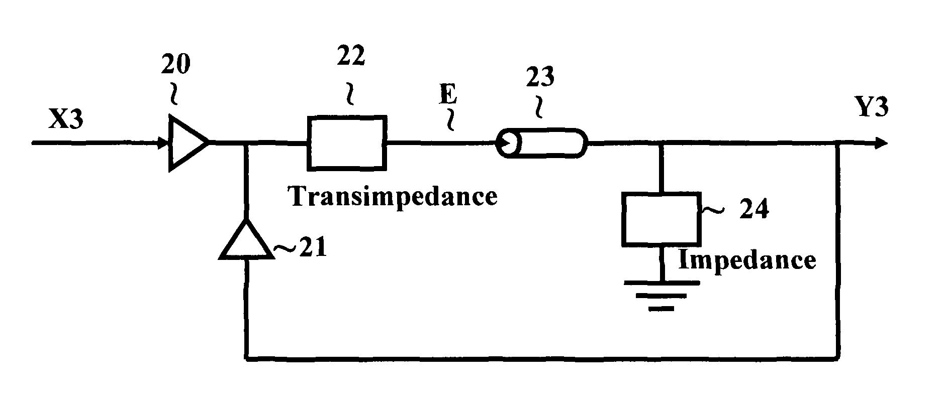
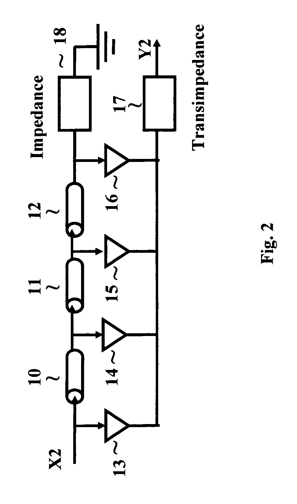
[0010]In general, implementations feature an analog filter circuit. The analog filter include a transmission line delay element and a transconductance element as a building block for fiber optic transmission systems, multi-gigahertz serial chip-to-chip communications, multi-gigahertz serial backplane communications, high-speed network communications, disk drive channel equalization, and filtering for radio frequency (RF) systems. In general, the transmission line delay element has a delay time and time-delays an input signal. The transmission delay line is terminated with a matched or mismatched impedance element according to the filter response requirement. In general, the transconductance element multiplies the time-delayed input signal by a tunable filter coefficient then converts the multiplied time-delayed input signal to a current. The analog filtering is performed by the multiplication function of the transconductance elements. A number of multiplied time-delayed input signals by different delay times of the transmission delay lines are converted to currents by the transconductance elements. The outputs of the transconductance elements couple together to form a current summing node to sum the multiplied or amplified different time-delayed currents into a summed current. In general, the summed current is converted back to a voltage signal by a transimpedance element to produce the filtered output voltage signal.
[0011]In general, the analog filter is configured to perform filtering functions, such as the IIR filtering. In other implementation, the analog filter is configured to perform FIR filtering functions.
[0012]These and other implementations can optionally include one or more of the following features. The input can also enter a no-delay transconductance element to be filtered and converted to a no-delay current before summed together with currents produced from different time-delayed input signals. A forward transmission delay line is configured to have at least one forward transmission line delay element for time-delaying the output signal by corresponding at least one forward delay time for using in FIR filtering. A feedback transmission delay line is configured to have at least one feedback transmission line delay element for time-delaying the output signal by corresponding at least one feedback delay time for using in IIR filtering. Each of the forward and feedback transmission delay lines is terminated with a matched or mismatched impedance element according to the filter response requirement. The forward and feedback transmission line delay elements can generate time-delayed input and output signals. The time-delayed input signal and the output signal and the no-delay input signal can be each multiplied by a corresponding transconductance element with a corresponding filter coefficient. The multiplied no-delay input signal, the multiplied time-delayed forward input signal and the multiplied feedback output signal can be converted to corresponding currents by the corresponding transconductance element. The at least one forward current, the at least one feedback current and the no-delay current can be summed into a summed current at the current summing node. A transimpedance amplifier couples to the current summing node to convert the summed node and generate an output voltage signal. The input signal and the output signal can be single ended or differential. In general, the filter coefficient is equal to the transconductance of the transconductance element and is tuned to respond to a system filter requirement specification. These and other implementations can optionally include one or more of the following features. A transconductance element can include a differential transistor pair. A differential gate terminal of the differential transistor pair can couple to the input signal and a differential source terminal of the differential transistor pair can couple to a ground or a negative power supply via a differential current source. A variable resistor can couple between the differential source terminal to tune the transconductance, therefore the filter coefficients of the transconductance element. The variable resistor can be a serial resistor network with a fixed and at least one switched resistor or a parallel resistor network with a fixed and at least one switched parallel resistor. The transimpedance element can be a pair load resistors coupled to the differential drain terminal of the transconductance element. The pair can be replaced by a transimpedance amplifier with feedback impedances to tune the transimpedance amplifier.
[0013]In general, the analog filter circuit is implemented according to a filter response requirement in selecting the number of delay elements, delay times of the delay elements, filter coefficients, gain of the amplifiers and layout considerations. An analog filter circuit can implement a variety of FIR filters including low pass filters, high pass filters, band pass filters, notch filters, differentiators, or comb filters. The forward FIR filter coefficients can be easily obtained by taking the Fourier Transform of the system filter response. An alaog filter circuit can implement a variety of IIR filters including low pass filters, high pass filters, band pass filters, notch filters, or integrators. The analog filter described can be implemented in high speed, i.e. 1 GHz to over 100 GHz, for equalization in fiber optic transmission systems, multi-gigahertz serial chip-to-chip communications, multi-gigahertz serial backplane communications, high-speed network communications, disk drive channel equalization, and filtering for radio frequency (RF) systems. The analog filter can be implemented on-chip, off-chip, on printed circuit board or on backplane.

