Method for manufacturing 3D circuits from bare die or packaged IC chips by microdispensed interconnections

a technology of interconnection and 3d circuit, which is applied in the direction of resistive material coating, solid-state device, printed inductance incorporation, etc., can solve the problems of general limitation of current 3d packaging and interconnection technology

Active Publication Date: 2011-07-05
SCIPERIO
View PDF5 Cites 33 Cited by
  • Summary
  • Abstract
  • Description
  • Claims
  • Application Information

AI Technical Summary

Problems solved by technology

The current 3D packaging and interconnection technology is generally limited to the tasks of producing the dense arrays of stacked memory or processing IC chips for the sake of increasing the capacity and processing power within the limited footprint on the printed circuit board.

Method used


Image

  • Method for manufacturing 3D circuits from bare die or packaged IC chips by microdispensed interconnections
  • Method for manufacturing 3D circuits from bare die or packaged IC chips by microdispensed interconnections
  • Method for manufacturing 3D circuits from bare die or packaged IC chips by microdispensed interconnections

Examples


Embodiment Construction

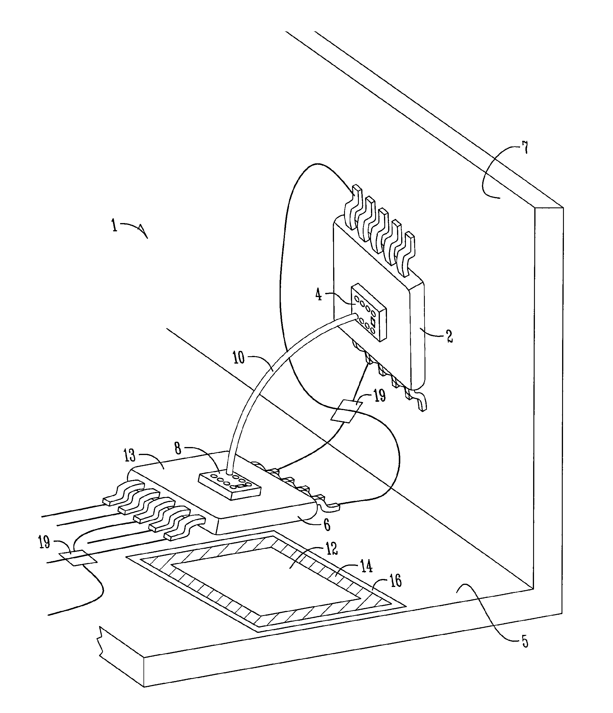
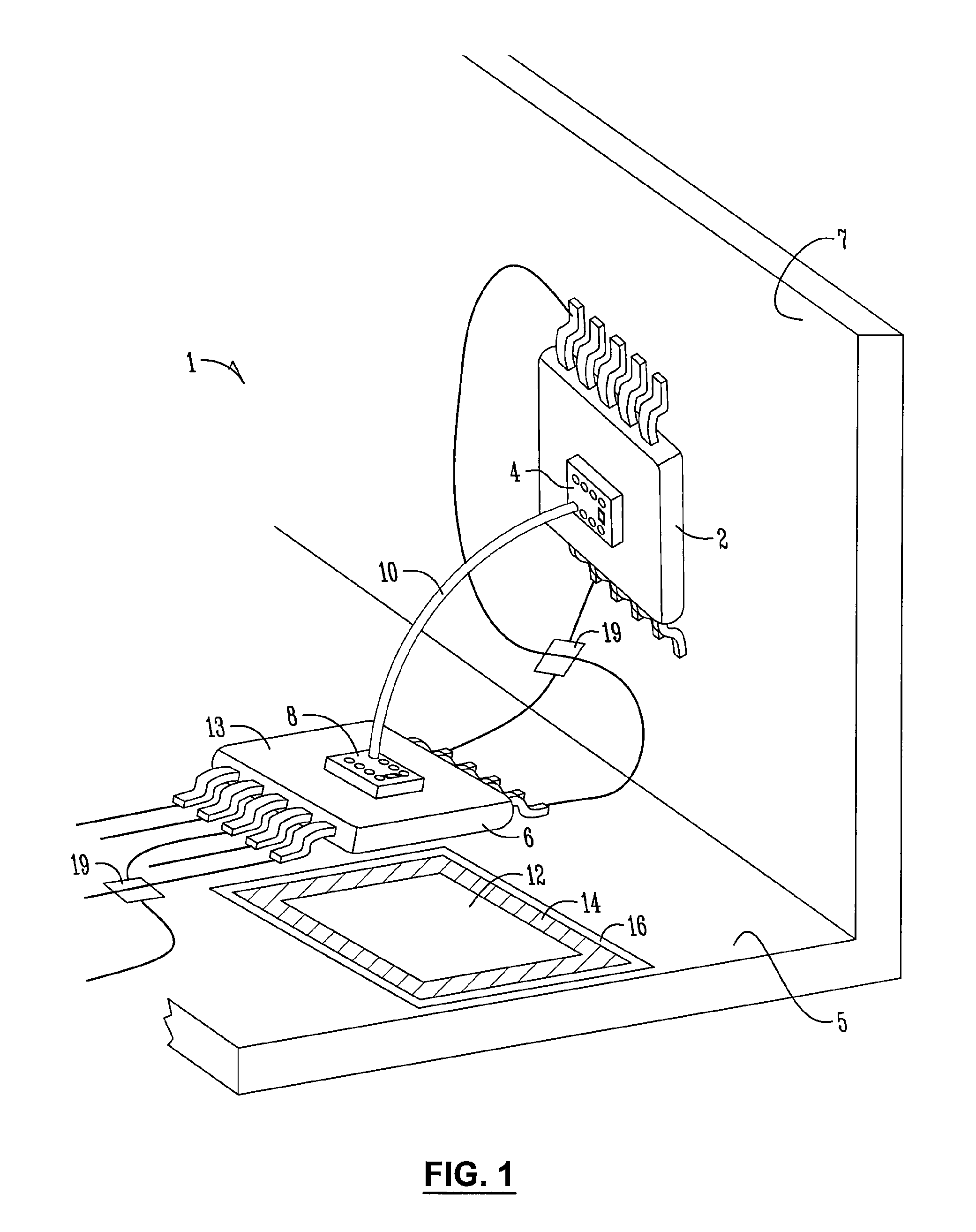
[0013]The present invention to improve upon the state of the art. The present invention provides for 3D packaging and interconnection. The present invention also provides for 3D packaging and interconnection in a manner beyond stacking of integrated circuit chips.

[0014]In addition, the present invention provides for 3D electronic circuits having small footprints and high volumetric density of components, and provides for improved cooling of heat generating components by enhanced heat exchange.

[0015]Further, the present invention provides for flexibility in a 3D electronic circuit such that the circuit may built where space is highly limited, on the conformal surfaces of solid or flexible substrates, or even without any substrate at all, directly on the sidewalls of the device enclosure or anywhere else on the skin or the structure of the hosting apparatus.

[0016]One or more of these and / or other objects, features, or advantages of the present invention will become apparent from the s...


PUM

PropertyMeasurementUnit
electricalaaaaaaaaaa
conductingaaaaaaaaaa
conductiveaaaaaaaaaa

Abstract

A method for manufacturing an electronic circuit in three-dimensional space provides for interconnecting electronic components within the circuit by directly writing conducting lines. The method may include observing a direct writing tool of a direct write system using a vision system, determining proper placement of the direct writing tool at least partially based on the step of observing, and directly writing conducting lines in three dimensions using the proper placement. The direct writing may be on a surface or in free space. The method may include stacking a plurality of chips to provide a stack having a top surface and edges extending away from the top and interconnecting connections of the chips by directly writing conducting lines along one of the edges.

Description

CROSS-REFERENCE TO RELATED APPLICATIONS[0001]This application claims the benefit of provisional patent application Ser. No. 60 / 595,542 filed Jul. 13, 2005, entitled THREE DIMENSIONAL ELECTRICAL CIRCUITS, the contents of which are hereby incorporated by reference in their entirety.FIELD OF THE INVENTION[0002]The present invention relates to the field of three dimensional electronic circuits manufactured from bare die or pre-packaged IC chips by direct written interconnections.BACKGROUND OF THE INVENTION[0003]The current 3D packaging and interconnection technology is generally limited to the tasks of producing the dense arrays of stacked memory or processing IC chips for the sake of increasing the capacity and processing power within the limited footprint on the printed circuit board. The current technological processes utilize the soldering connections of the pre-aligned arrays of the designated contact pads by dipping the edge of the stack into a vat of molten solder or by re-flowin...

Claims


Application Information

Patent Timeline
Patent Type & Authority Patents(United States)
IPC IPC(8): B05D5/12B05D3/00
CPCH01L21/4867H01L24/24H01L24/25H01L24/82H01L25/03H01L25/065H01L25/0657H01L2224/2401H01L2224/24011H01L2224/24051H01L2224/24147H01L2224/245H01L2224/25175H01L2224/82101H01L2224/82801H01L2224/82874H01L2224/82948H01L2224/82986H01L2225/06541H01L2225/06551H01L2225/06565H01L2924/14H05K1/0284H05K1/162H05K1/165H05K1/167H05K3/125H05K2201/10515H05K2201/1053H05K3/3485H01L2924/00012H01L2924/06H01L2924/00
Inventor CHURCH, KENNETH H.CLARK, PATRICKXU, DONGJIANGSWAN, LANCEIRWIN, BRYANPELEKHATY, VLADIMIR
Owner SCIPERIO
Why Eureka
Try Eureka