Reference voltage generation circuit and start-up control method therefor
a reference voltage and start-up control technology, which is applied in the direction of process and machine control, ac network circuit arrangement, instruments, etc., can solve the problems of internal circuit connected to the output terminal vo, output voltage vo exceeding the set, and takes a long time to complete the charging of the capacitor c of the start-up circuit, etc., to prevent the output voltage from exceeding, rapid start-up, and rapid start-up
- Summary
- Abstract
- Description
- Claims
- Application Information
AI Technical Summary
Benefits of technology
Problems solved by technology
Method used
Image
Examples
first exemplary embodiment
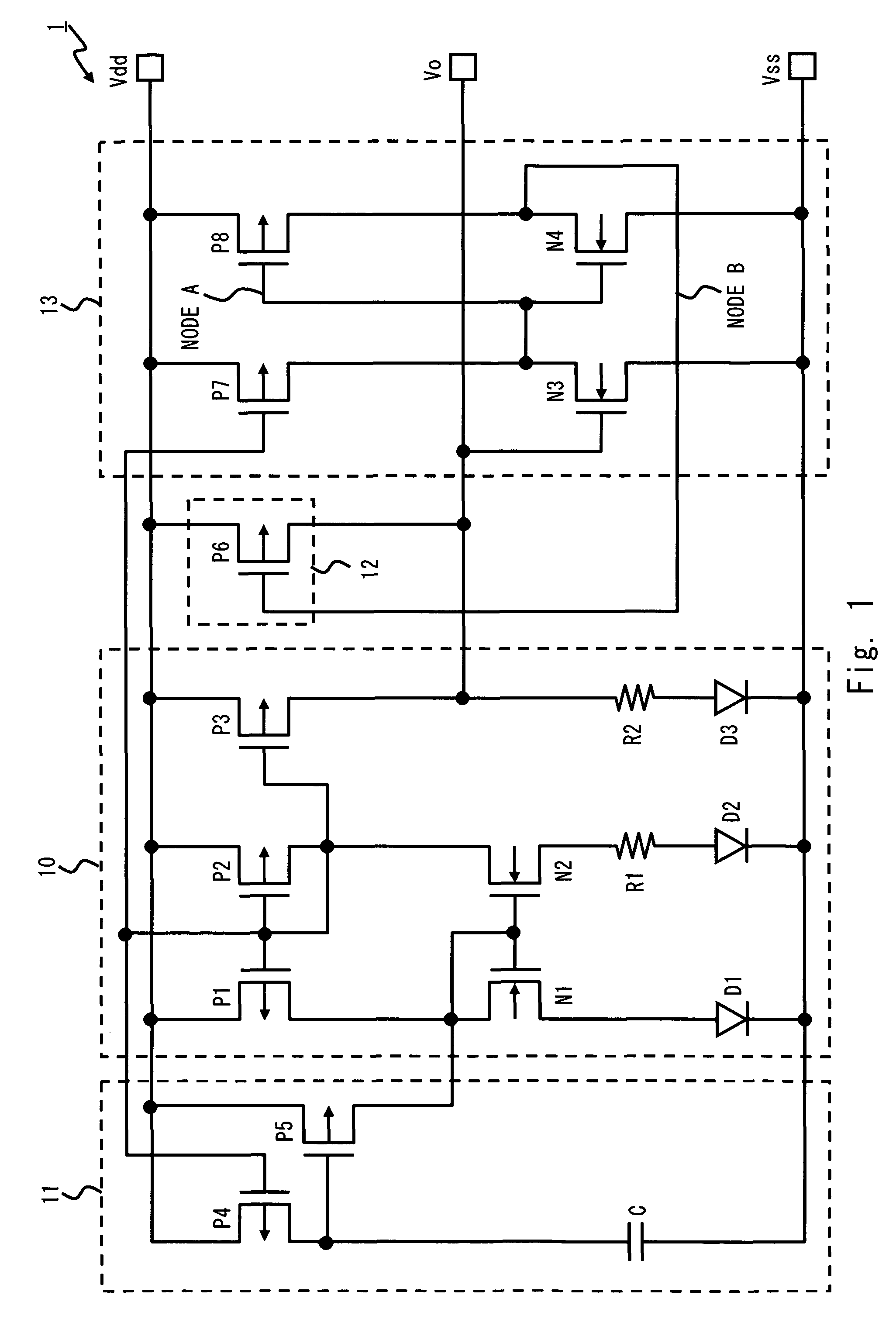
[0023]Hereinafter, exemplary embodiments of the present invention will be described with reference to the accompanying drawings. FIG. 1 shows a block diagram of a reference voltage generation circuit 1. As shown in FIG. 1, the reference voltage generation circuit 1 includes a voltage generation circuit 10, a start-up circuit 11, an auxiliary start-up circuit 12, and a control circuit 13.
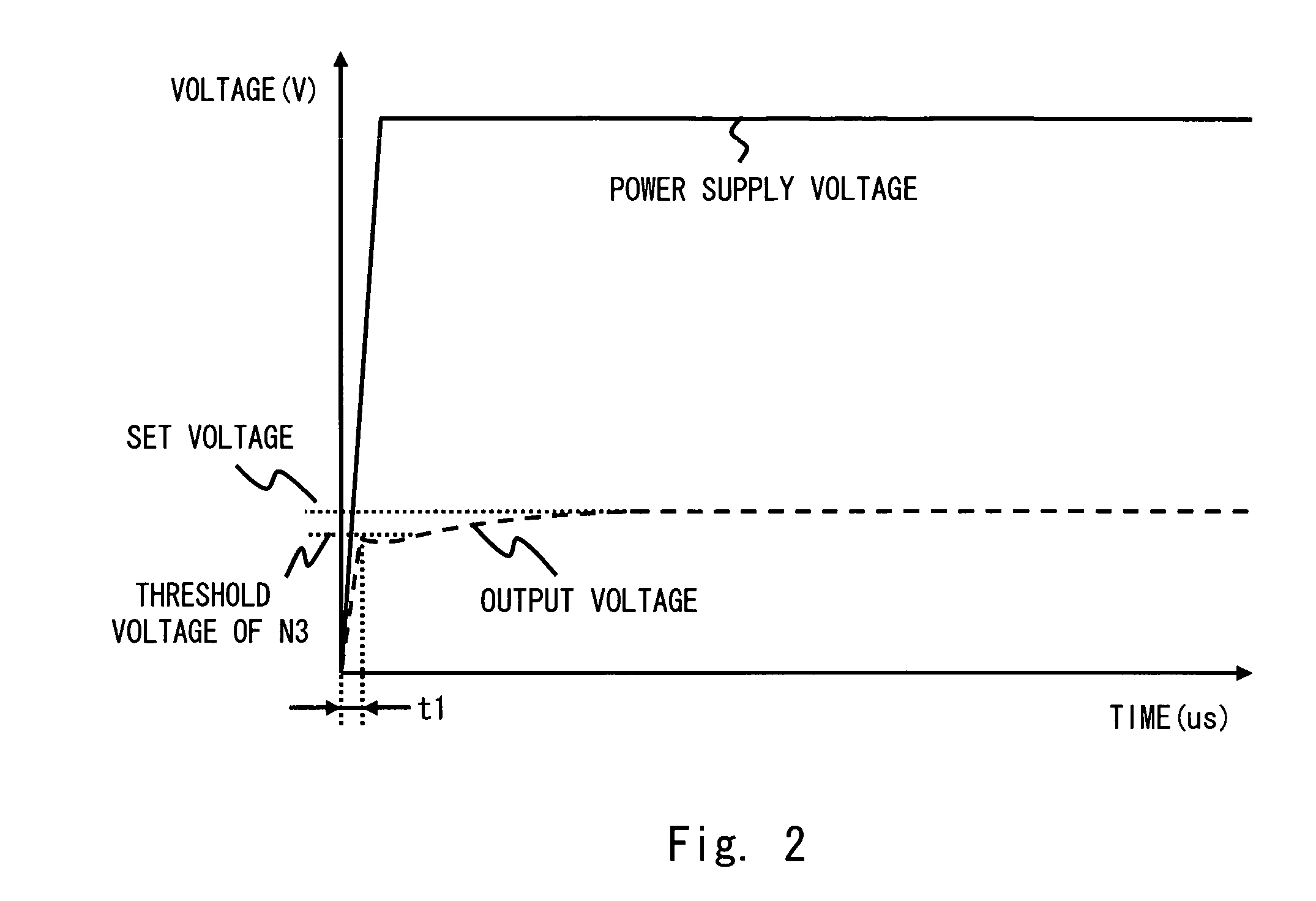
[0024]The voltage generation circuit 10 outputs a reference voltage having a voltage value equal to that of a preset voltage. The voltage generation circuit 10 includes PMOS transistors P1 to P3, NMOS transistors N1 and N2, resistors R1 and R2, and diodes D1 to D3. The start-up circuit 11 assists the operation of the voltage generation circuit 10 after power-on. The start-up circuit 11 includes PMOS transistors P4 and P5 and a capacitor C. The auxiliary start-up circuit 12 assists the rise of an output voltage output from an output node of the voltage generation circuit 10. The auxiliary start-up cir...
second exemplary embodiment
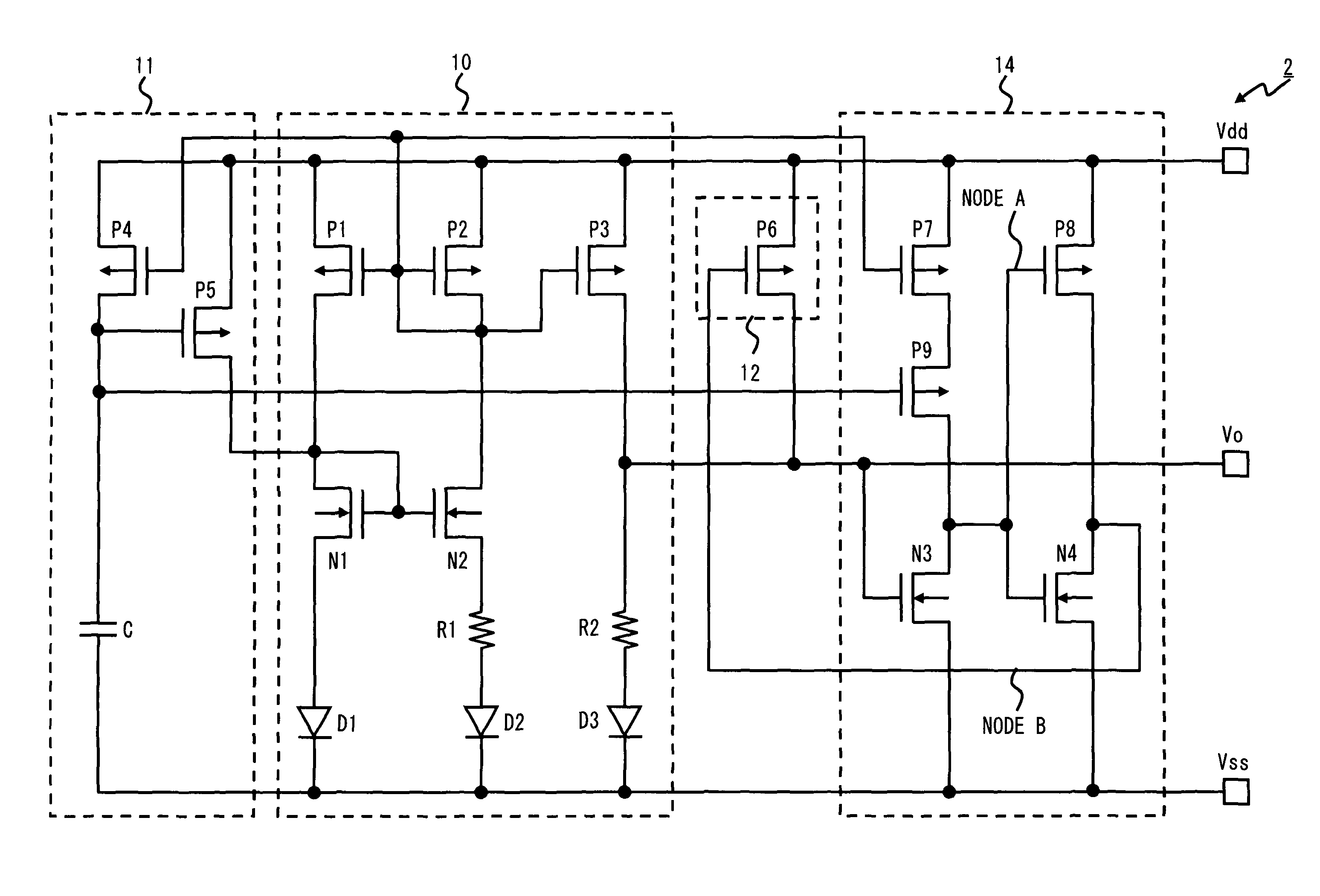
[0040]FIG. 3 shows a circuit diagram of a reference voltage generation circuit 2 according to a second exemplary embodiment of the present invention. As shown in FIG. 3, the reference voltage generation circuit 2 includes a control circuit 14 which is obtained by adding a PMOS transistor P9 to the control circuit 13. In the control circuit 13, in the state where the output voltage of the reference voltage generation circuit 1 reaches the set voltage, the NMOS transistor N3 is rendered conductive and the PMOS transistor P7 is also rendered conductive. Accordingly, in the control circuit 13, in the state where the output voltage of the reference voltage generation circuit 1 reaches the set voltage, a flow-through current flows from the power supply terminal Vdd to the ground terminal Vss through the PMOS transistor P7 and the NMOS transistor N3. The PMOS transistor P9 prevents the flow-through current from flowing.
[0041]The PMOS transistor P9 has a source terminal connected to the dra...
PUM
 Abstract
Description
Claims
Application Information


