
Vertical channel transistors and memory devices including vertical channel transistors

a technology of vertical channel transistor and transistor, which is applied in the direction of transistors, semiconductor devices, electrical apparatus, etc., can solve the problems of difficult to realize a cmos operation mode using conventional nmos vertical channel transistors, and difficult to accurately and reliably implant impurities into the pillar-like structure of p-type and n-type vertical channel layers

Inactive Publication Date: 2011-07-12
SAMSUNG ELECTRONICS CO LTD
View PDF25 Cites 47 Cited by
  • Summary
  • Abstract
  • Description
  • Claims
  • Application Information

AI Technical Summary

Benefits of technology

The present invention provides a semiconductor device that includes a memory core area with a plurality of NMOS vertical channel select transistors and a plurality of PMOS vertical channel transistors. The NMOS transistors have a p+ poly-silicon gate electrode surrounding a vertical p-channel region, while the PMOS transistors have a n+ poly-silicon gate electrode surrounding a vertical n-channel region. The semiconductor device also includes a sense amplifier with a plurality of NMOS and PMOS transistors. The technical effect of this invention is to provide a semiconductor device with improved performance and reliability.

Problems solved by technology

One drawback of vertical channel transistors is that it is difficult to accurately and reliably implant impurities into the pillar-like structures of the p-type and n-type vertical channel layers 302 and 312.
This is especially problematic with respect to the NMOS vertical channel transistor.
However, any attempt to implant ions in the p-type vertical channel 302 will likely result in a non-uniform ion density distribution, which can cause intended variations in the threshold voltage Vth.
In addition, it is difficult to realize a CMOS operational mode using conventional NMOS vertical channel transistors, since a CMOS operational mode generally requires a positive threshold for the NMOS transistors.

Method used


Image

  • Vertical channel transistors and memory devices including vertical channel transistors
  • Vertical channel transistors and memory devices including vertical channel transistors
  • Vertical channel transistors and memory devices including vertical channel transistors

Examples


Embodiment Construction

[0028]The invention is described more fully hereinafter with reference to the accompanying drawings, in which exemplary embodiments of the present invention are shown. The present invention may, however, be embodied in many different forms and should not be construed as limited to the examples set forth herein. In the drawings, the sizes and relative sizes of layers and regions may be exaggerated and / or simplified for clarity. Also, it will be understood that when an element or layer is referred to as being “on”, “connected to” or “coupled to” another element or layer, it can be directly on, connected or coupled to the other element or layer, or intervening elements or layers may be present.

[0029]The present invention will now be described by way of preferred, but non-limiting, embodiments of the invention.

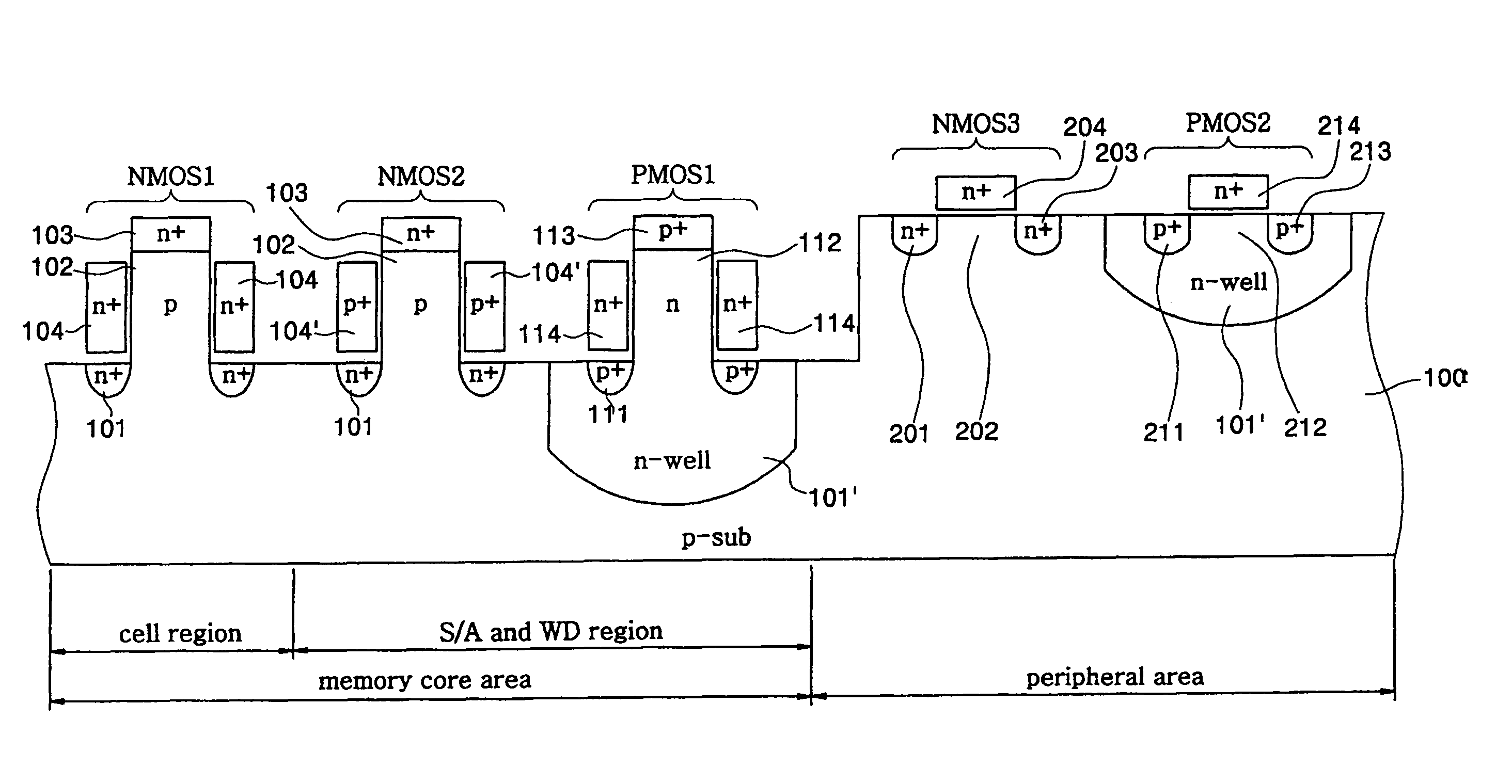
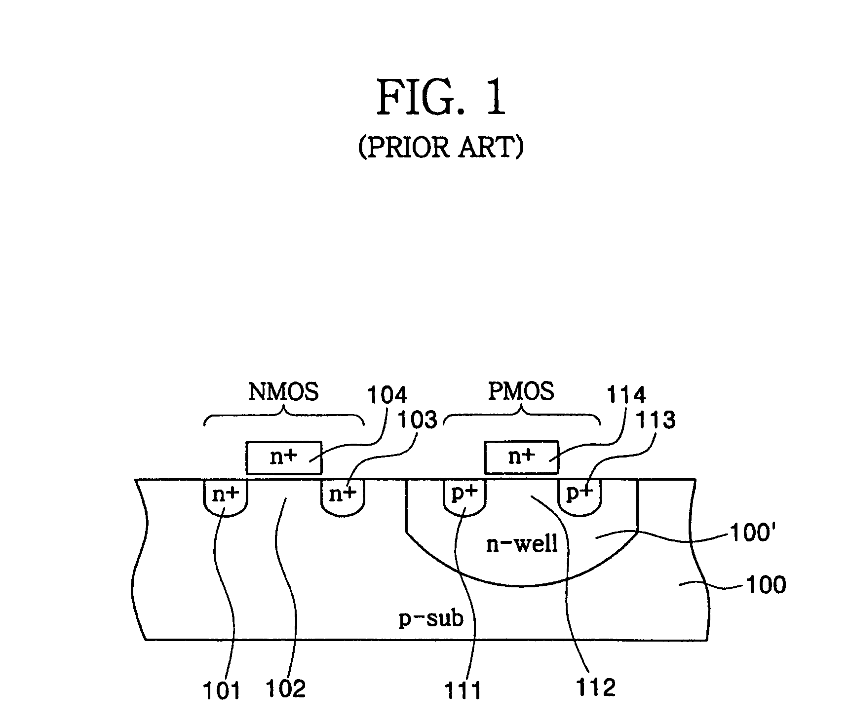
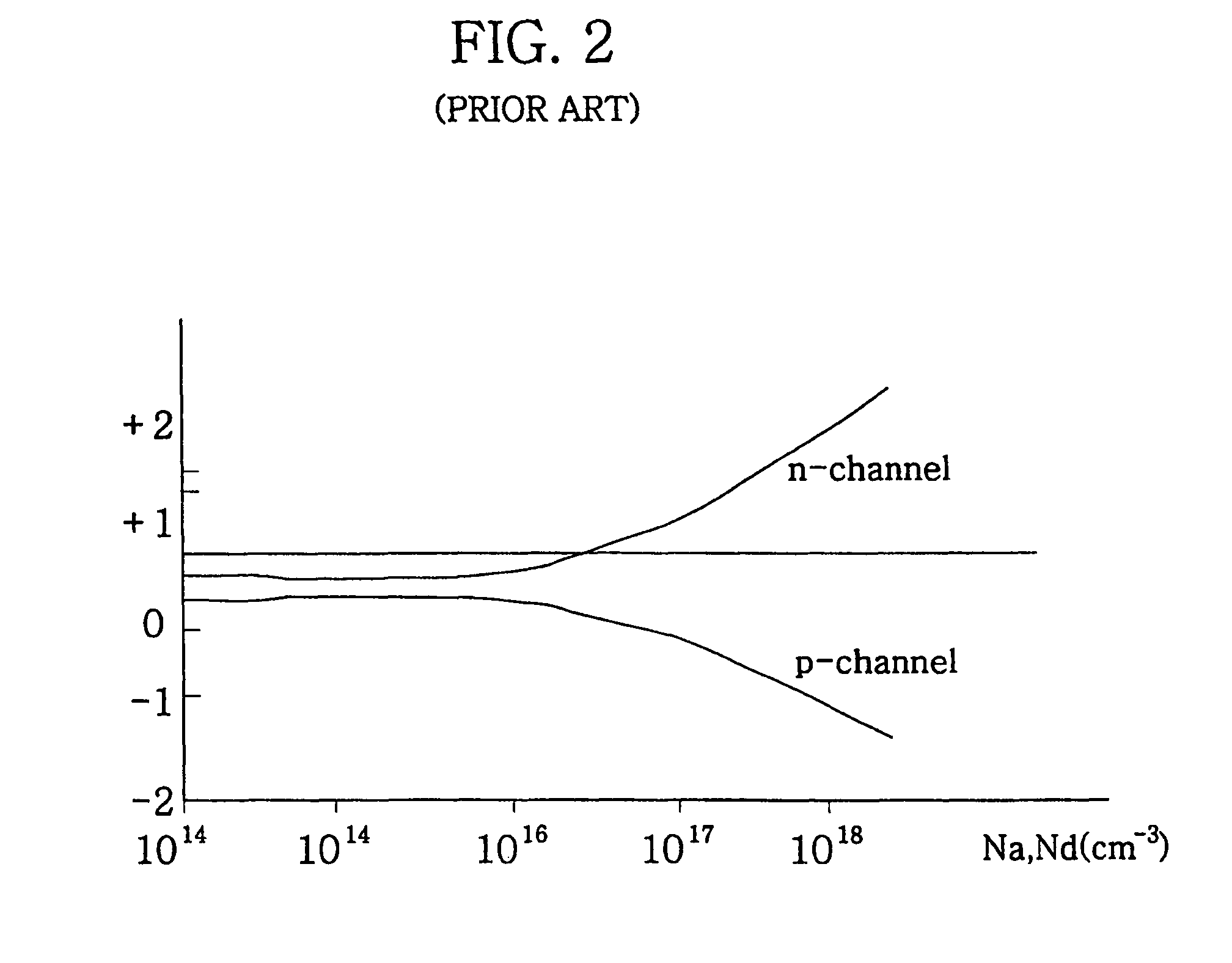
[0030]FIG. 4 is a cross-sectional schematic view of a semiconductor device according to an embodiment of the present invention. As illustrated, the semiconductor device of this ex...


PUM


Abstract

A semiconductor device is provided which includes an NMOS vertical channel transistor located on a substrate and including a p+ polysilicon gate electrode surrounding a vertical p-channel region, and a PMOS vertical channel transistor located on the substrate and including an n+ polysilicon gate electrode surrounding a vertical n-channel region. The NMOS and PMOS vertical channel transistors are optionally operable in a CMOS operational mode.

Description

BACKGROUND OF THE INVENTION[0001]1. Field of the Invention[0002]The present invention generally relates to semiconductor devices, and more particularly, the present invention relates to vertical channel transistors and semiconductor memory devices which include vertical channel transistors.[0003]2. Description of the Related Art[0004]FIG. 1 is a schematic cross-sectional view of the PMOS and NMOS planar channel transistors of a conventional CMOS device. As illustrated, the NMOS planar channel transistor is generally defined by n+ type source / drain regions 101 and 103 formed in the surface of a p-type substrate 100, and an n+ type poly-silicon gate electrode 104 is located over an p-channel region 102 of the NMOS planar channel transistor. The PMOS planar channel transistor is generally defined by p+ type source / drain regions 111 and 113 formed in the surface of an n-type well 100′ of p-type substrate 100. An n+ type poly-silicon gate electrode 114 is located over a n-channel region ...

Claims


Application Information

Patent Timeline
Patent Type & Authority Patents(United States)
IPC IPC(8): H01L29/66
CPCH01L21/823842H01L21/823885H01L27/092H01L27/105H01L27/1052H10B99/22H01L29/7827
Inventor KIM, JIN-YOUNGSONG, KI-WHAN
Owner SAMSUNG ELECTRONICS CO LTD
Features
  • Generate Ideas
  • Intellectual Property
  • Life Sciences
  • Materials
  • Tech Scout
  • Unparalleled Data Quality
  • Higher Quality Content
  • 60% Fewer Hallucinations
Learn More