Semiconductor device having SiGe semiconductor regions
a semiconductor region and semiconductor technology, applied in the field of semiconductor devices, can solve problems such as difficulty in applying sufficient stress to the channel region
- Summary
- Abstract
- Description
- Claims
- Application Information
AI Technical Summary
Benefits of technology
Problems solved by technology
Method used
Image

Examples
embodiment 1
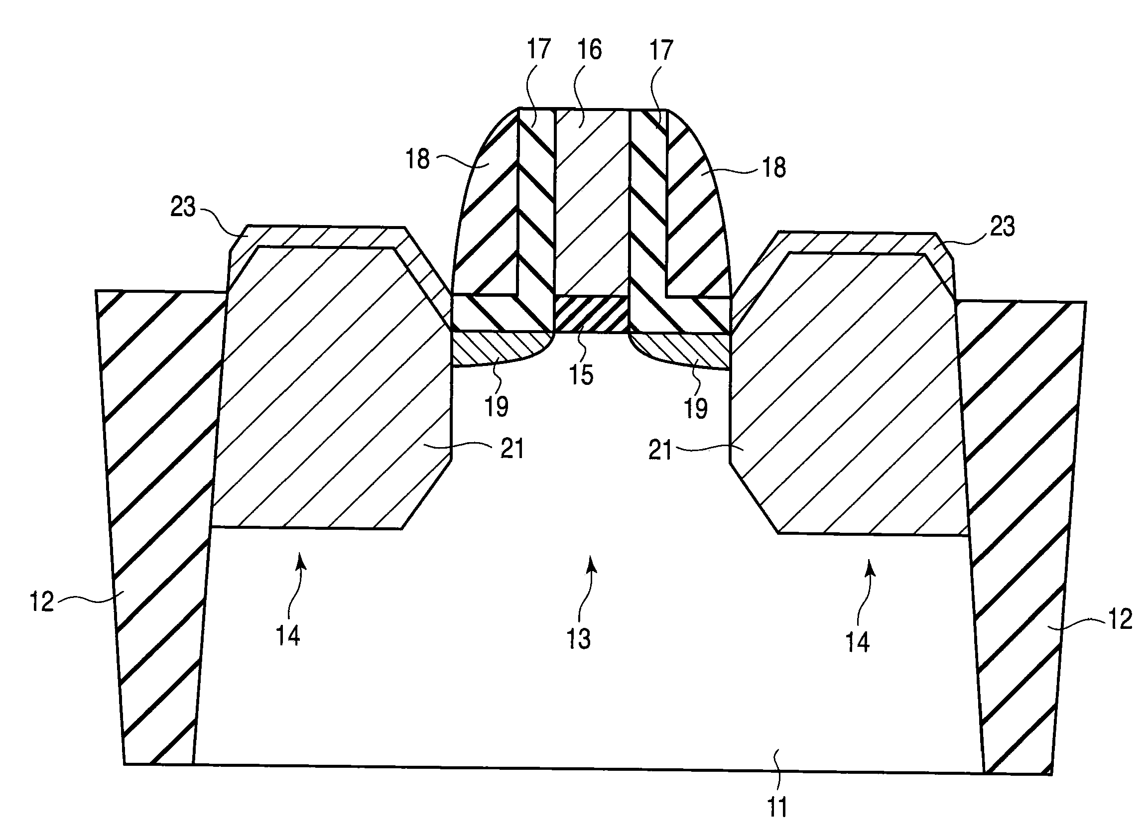
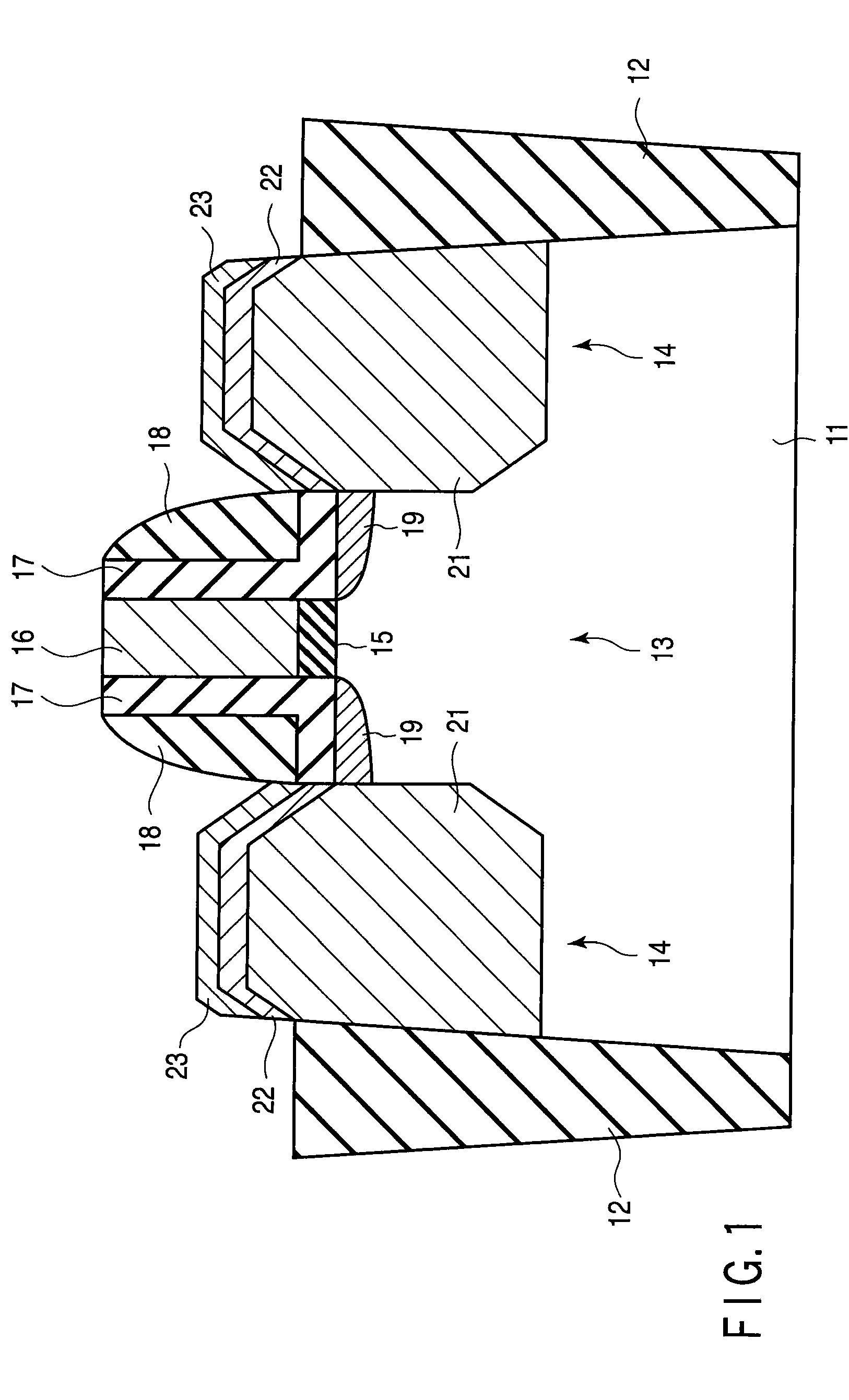
[0015]FIG. 1 is a cross-sectional view schematically showing the structure of a semiconductor device according to a first embodiment of the present invention.
[0016]As shown in FIG. 1, the surface area of a silicon substrate (semiconductor substrate) 11 is formed with an isolation insulating region 12. A p-type MIS transistor is formed at an element region surrounded by the isolation insulating region 12.
[0017]The element region includes a first semiconductor region 13 having a channel region. The first semiconductor region 13 corresponds to a convex-shaped region defined by a trench 14. A gate insulating film 15 is formed on the first semiconductor region 13. A gate electrode 16 is formed on the gate insulating film 15. The sidewall of the gate electrode 16 is formed with a sidewall oxide film (silicon oxide film) 17 and a sidewall nitride film (silicon nitride film) 18. The first semiconductor region 13 is formed with extension regions 19 containing p-type impurity at the vicinity ...
embodiment 2
[0042]A semiconductor device according to a second embodiment of the present invention will be hereinafter described. In this case, the basic structure and manufacturing method are the same as the first embodiment. Thus, an explanation about the matters described in the first embodiment is omitted. The drawing uses FIG. 1 shown in the first embodiment.
[0043]According to this embodiment, a cap layer 22 is formed of SiGe containing carbon (C). The carbon concentration of the cap layer 22 is lower than the germanium concentration of a second semiconductor region 21. More specifically, the carbon concentration of the cap layer 22 is sufficiently lower than 1 / 10 of the germanium concentration of a second semiconductor region 21. Other basic structure is the same as the first embodiment. Specifically, a silicide layer 23 is formed of nickel silicide (Ni silicide) or nickel-platinum alloy silicide (Ni—Pt alloy silicide). Usually, the silicide layer 23 contains carbon, but does not substant...
embodiment 3
[0046]A semiconductor device according to a third embodiment of the present invention will be hereinafter described. In this case, the basic structure and manufacturing method are the same as the first embodiment. Thus, an explanation about the matters described in the first embodiment is omitted.
[0047]FIG. 5 is a cross-sectional view schematically showing the structure of a semiconductor device according to a third embodiment. The basic structure of the semiconductor device shown in FIG. 5 is the same as shown in FIG. 1. The same reference numerals are used to designate portions corresponding to FIG. 1, and the details are omitted.
[0048]According to this embodiment, a second semiconductor region 21 formed of SiGe contains carbon, and the carbon concentration increases in the thickness direction of the second semiconductor region 21. In other words, the carbon concentration increases from the bottom portion of the second semiconductor region 21 toward the top portion thereof. The ca...
PUM
| Property | Measurement | Unit |
|---|---|---|
| thickness | aaaaa | aaaaa |
| temperature | aaaaa | aaaaa |
| temperature | aaaaa | aaaaa |
Abstract
Description
Claims
Application Information
 - R&D
- Intellectual Property
- Life Sciences
- Materials
- Tech Scout
- Unparalleled Data Quality
- Higher Quality Content
- 60% Fewer Hallucinations
Browse by: Latest US Patents, China's latest patents, Technical Efficacy Thesaurus, Application Domain, Technology Topic, Popular Technical Reports.
© 2025 PatSnap. All rights reserved.Legal|Privacy policy|Modern Slavery Act Transparency Statement|Sitemap|About US| Contact US: help@patsnap.com