Transistor having V-shaped embedded stressor

a stressor and transistor technology, applied in the field of semiconductor devices, can solve the problems of reducing the power consumption of chips, posing practical design challenges, and difficult to perform a correct linkup implant to electrically

Inactive Publication Date: 2011-08-02
ADVANCED MICRO DEVICES INC +1
View PDF7 Cites 27 Cited by
  • Summary
  • Abstract
  • Description
  • Claims
  • Application Information

AI Technical Summary

Problems solved by technology

Reduced power consumption on chips is another crucial issue that drives innovation in this area.
The prior art PFET design as shown in FIG. 1 can pose practical design challenges.
If a SiGe buffer layer having a germanium concentration below the germanium concentration of the stressor regions 135 is disposed between the extension regions and the stressor regions, it can be difficult to perform a correct linkup implant to electrically connect the extension region, the buffer layer and the stressor region.

Method used


Image

  • Transistor having V-shaped embedded stressor
  • Transistor having V-shaped embedded stressor
  • Transistor having V-shaped embedded stressor

Examples


Embodiment Construction

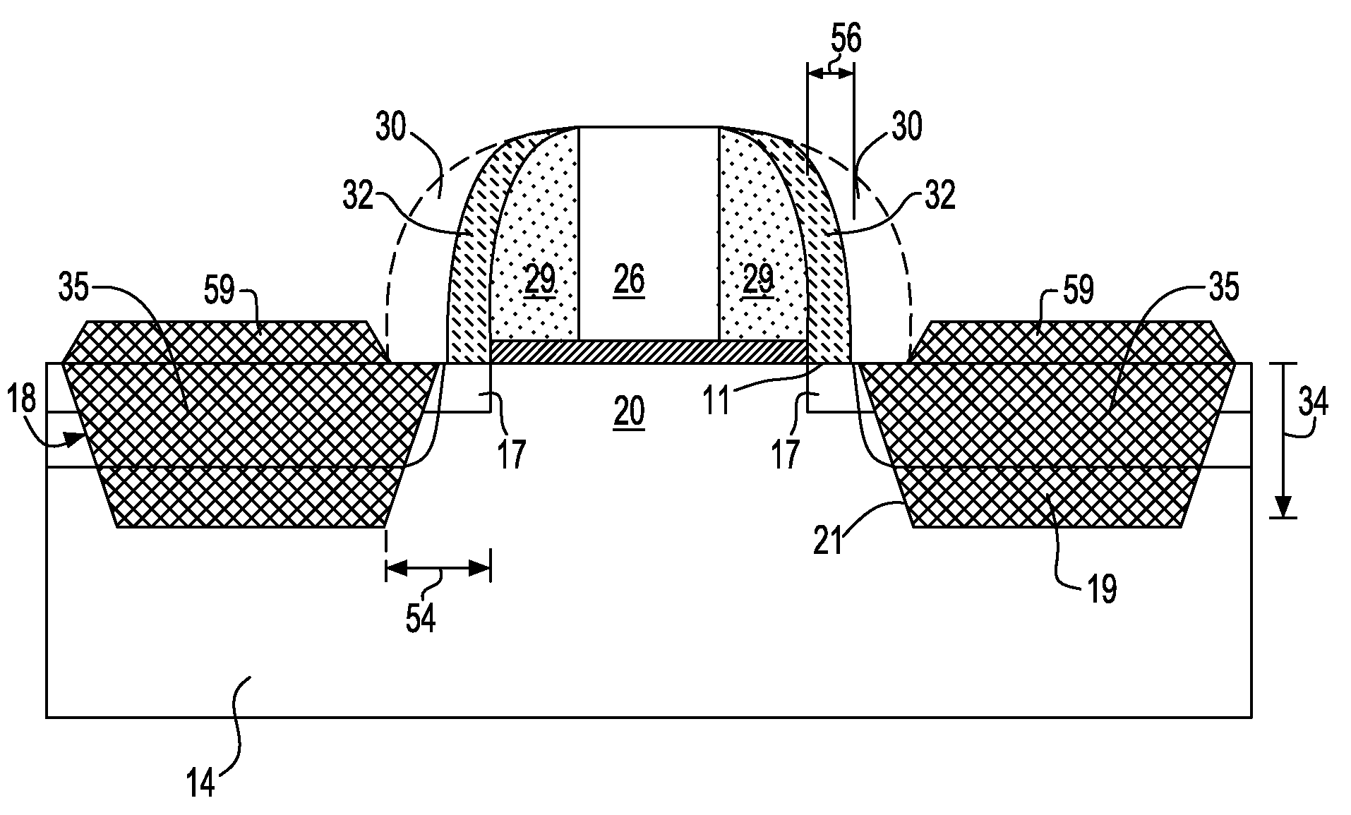
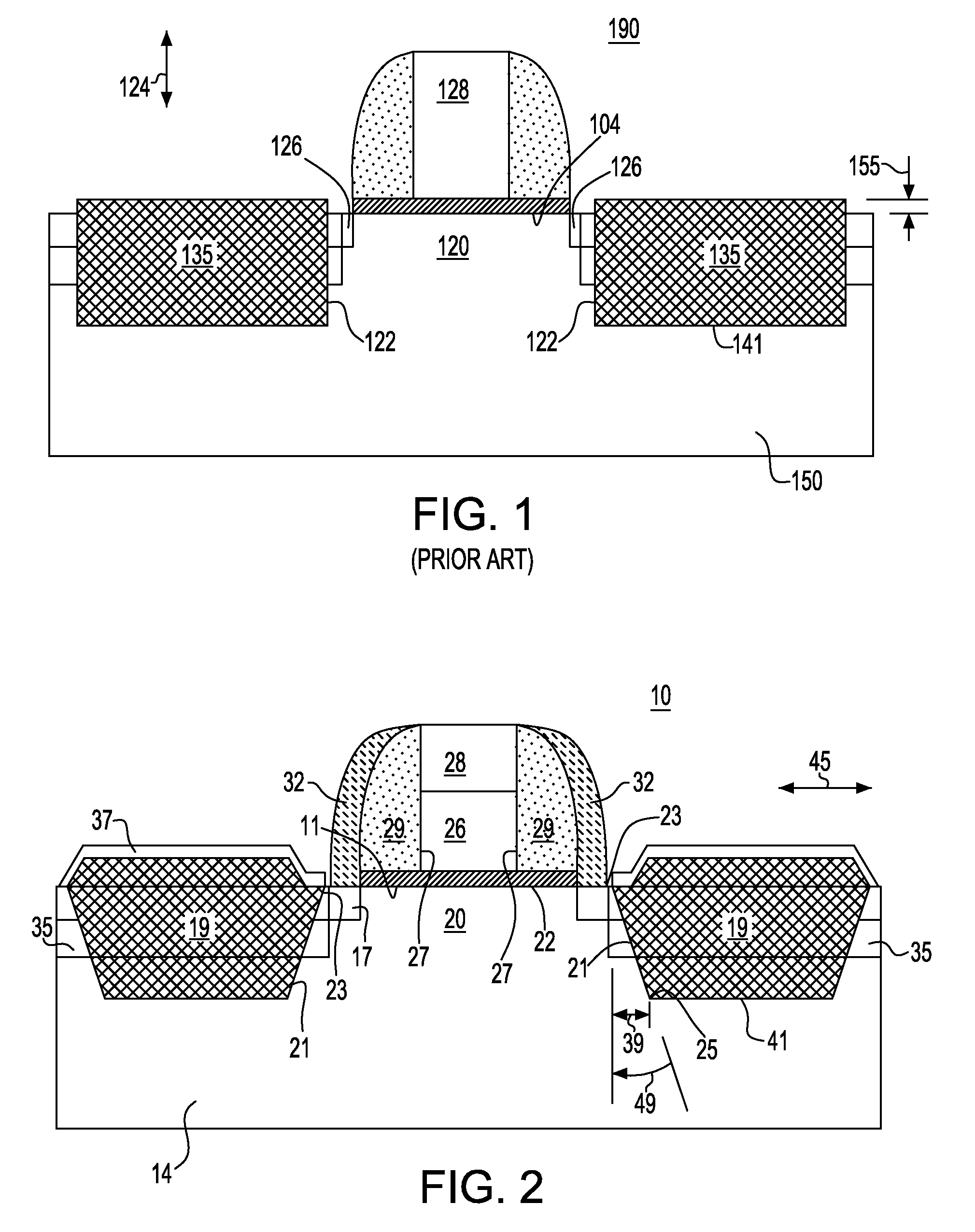
[0020]FIG. 2 is a sectional view illustrating a p-type field effect transistor (PFET) 10 according to one embodiment of the present invention. As illustrated in FIG. 2, the PFET 10 can have a conduction path provided in a mono crystalline semiconductor region of a substrate 14. The substrate 14 may either be a bulk substrate or can be a semiconductor-on-insulator or silicon-on-insulator (SOI) substrate in which a relatively thin layer of a mono crystalline semiconductor is formed over an insulating layer (not shown). When field effect transistors (FETs) are formed in such SOI substrates, faster switching operation is often achieved than otherwise, because junction capacitance between the channel region of the transistor and the bulk substrate can be eliminated. As described in this and the embodiments to follow, reference will be made to fabrication of transistors within a monocrystalline region of a substrate consisting essentially of silicon, which can have embedded stressor regio...


PUM


Abstract

A semiconductor device and a method of making the device are provided. The method can include forming a gate conductor overlying a major surface of a monocrystalline semiconductor region and forming first spacers on exposed walls of the gate conductor. Using the gate conductor and the first spacers as a mask, at least extension regions are implanted in the semiconductor region and dummy spacers are formed extending outward from the first spacers. Using the dummy spacers as a mask, the semiconductor region is etched to form recesses having at least substantially straight walls extending downward from the major surface to a bottom surface, such that a substantial angle is defined between the bottom surface and the walls. Subsequently, the process is continued by epitaxially growing regions of stressed monocrystalline semiconductor material within the recesses. Then the dummy spacers are removed and the transistor can be completed by forming source / drain regions of the transistor that are at least partially disposed in the stressed semiconductor material regions.

Description

BACKGROUND OF THE INVENTION[0001]1. Field of the Invention[0002]The present invention relates to semiconductor devices and their manufacture, and more specifically to a structure and method of making a field effect transistor (FET) having an embedded stressor.[0003]2. Description of the Related Art[0004]The industry trend in semiconductor technology is to create smaller devices that are faster than their predecessors. Reduced power consumption on chips is another crucial issue that drives innovation in this area. In this regard, complementary-metal-oxide-semiconductor (CMOS) circuits have become prevalent because of reduced power requirement and size. CMOS circuits often use a combination of p-type and n-type metal-oxide-semiconductor field effect transistors (MOSFETS) to implement logic gates and other circuit functions. It has been found that improved performance and reduced power requirement can be obtained when a stress is applied to the channel region of a MOSFET transistor to ...

Claims


Application Information

Patent Timeline
Patent Type & Authority Patents(United States)
IPC IPC(8): H01L21/336H01L21/76
CPCH01L29/165H01L29/6653H01L29/6656H01L29/66636H01L29/7834H01L29/7848H01L29/6659
Inventor CHAN, KEVIN K.GREENE, BRIAN J.HOLT, JUDSON R.JOHNSON, JEFFREY B.KANARSKY, THOMAS S.KOSHY, JOPHY S.MCSTAY, KEVINPARK, DAE-GYUWEIJTMANS, JOHAN W.YANG, FRANK B.
Owner ADVANCED MICRO DEVICES INC
Why Eureka
Try Eureka