Semiconductor device

a semiconductor device and on-resistance technology, applied in the field of semiconductor devices, can solve the problems of increasing the collector resistance, increasing the on-resistance of the hfet, and the semiconductor device described in the patent reference 1 cannot satisfy both of the characteristic advantages, so as to reduce the number of masks, reduce the on-resistance of the hfet, and reduce the mask length

Active Publication Date: 2011-09-13
PANASONIC SEMICON SOLUTIONS CO LTD
View PDF11 Cites 2 Cited by
  • Summary
  • Abstract
  • Description
  • Claims
  • Application Information

AI Technical Summary

Benefits of technology

[0015]This structure allows the cap layer of the HFET to include the external sub-collector region, and collector part to include the internal sub-collector region. Accordingly, the present invention can provide a single semiconductor layer to be shared with sub-collector layer of the HBT and the cap layer of the HFET, which leads to reduction of the number of masks in a manufacturing process of the semiconductor device. Further, this structure allows: the cap layer to be thin with the external sub-collector region thinned and with the sub-collector layer eliminating the need to be thin in the collector part; and the recess length of the HFET to be reduced. Accordingly, the present invention can reduce the on-resistance of the HFET. In addition, this structure allows the internal sub-collector region to be thick with the cap layer eliminating the need to be thick, and the collector resistance of the HBT to be reduced. Accordingly, the present invention can reduce the on-resistance of the HBT. As a result, the present invention can implement a semiconductor device satisfying both of the trade-off characteristic advantages between the HBT and the HFET, dispensing with an increase in the number of masks required for forming the Bi-HFET.
[0017]This manufacturing method allows a single mask process to process portion of the sub-collector layer, the collector layer, the base layer, and the emitter layer in a mesa shape in order to form the collector part. Accordingly, the present invention can manufacture a high-performance Bi-HFET, dispensing with an increase in the number of processes.
[0018]The present invention makes possible manufacturing of a Bi-HFET realizing both of a low-resistance HBT and a low-resistance HFET, eliminating the need for an increase in the number of masks required for the manufacturing thereof. Therefore, the present invention can result in achieving a low-cost and high-performance Bi-HFET and providing a significant contribution to commercial availability of Bi-HFETS.FURTHER INFORMATION ABOUT TECHNICAL BACKGROUND TO THIS APPLICATION

Problems solved by technology

The semiconductor device described in Patent Reference 1 causes a problem described hereinafter in satisfying both of the characteristic trade-off advantages between the HBT and the HFET.
In other words, the 300 nm-thickness of the GaAs sub-collector layer 407 causes a problem to increase a collector resistance.
Meanwhile, the 300 nm-thickness of the GaAs cap layer 405 causes a problem to increase the on-resistance of the HFET.
Thus, even the semiconductor device described in Patent Reference 1 cannot satisfy both of the characteristic advantages of the HBT and the HFET.

Method used


Image

  • Semiconductor device
  • Semiconductor device
  • Semiconductor device

Examples


Embodiment Construction

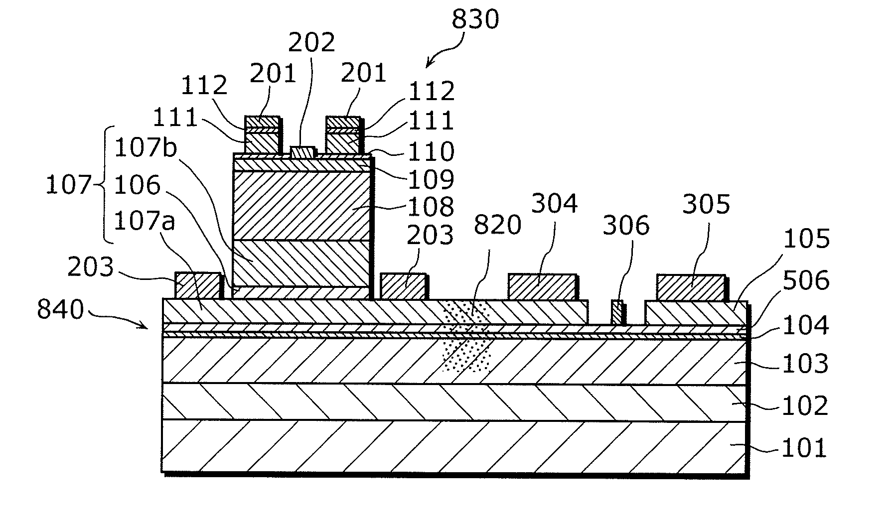
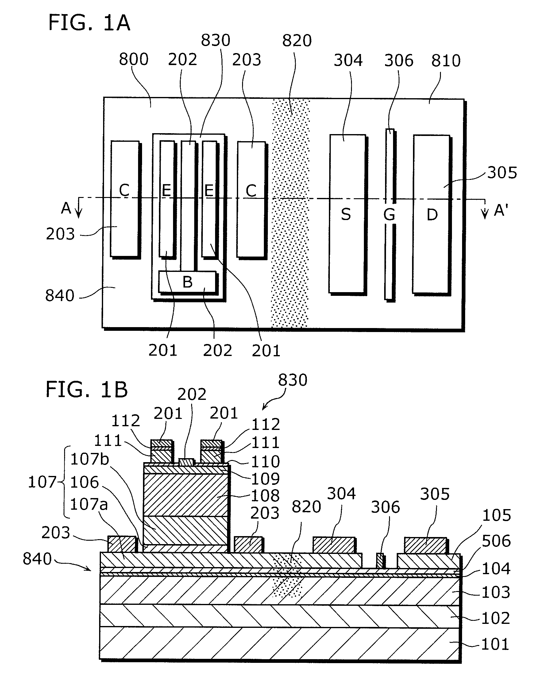
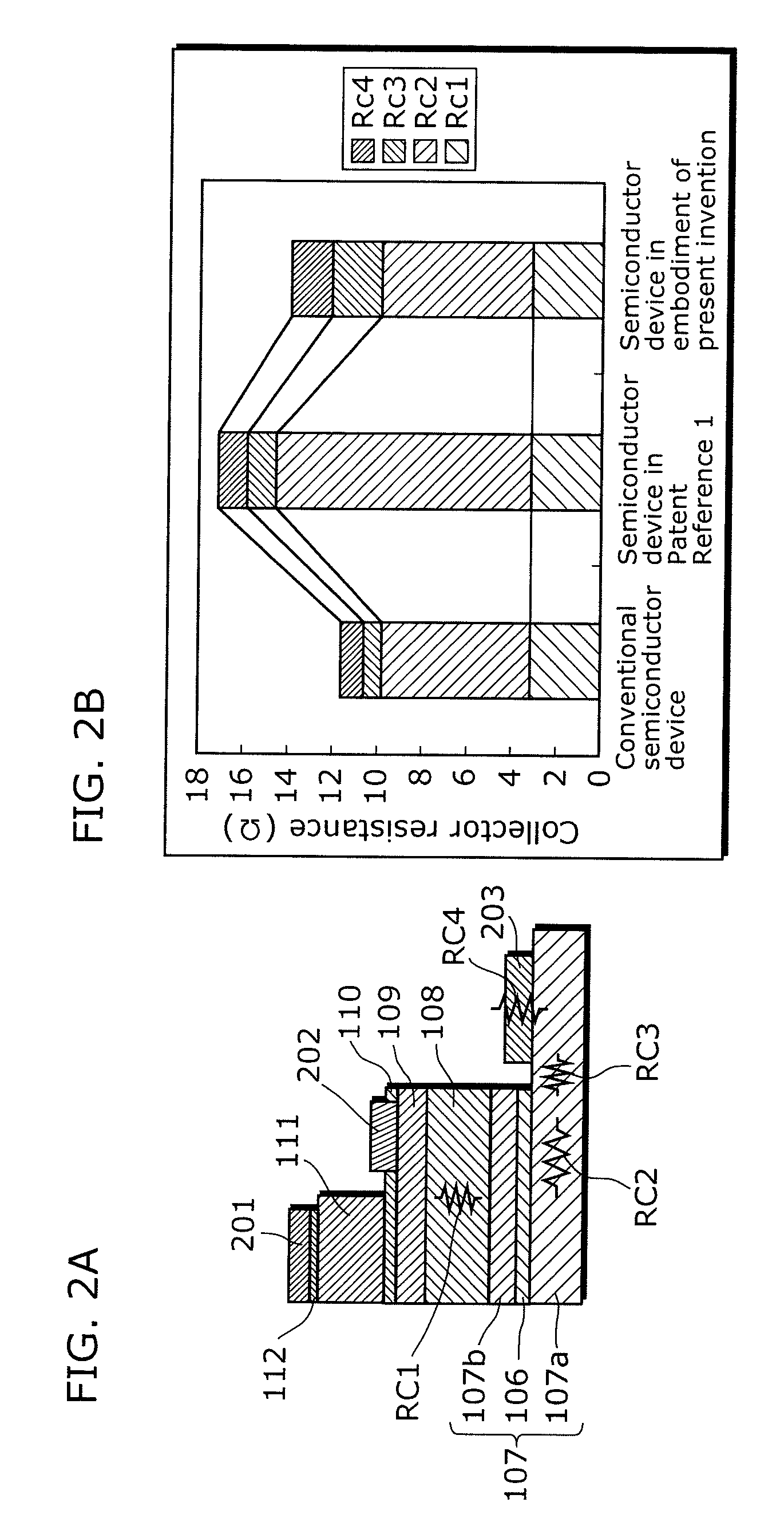
[0027]Hereinafter, an HBT and HFET integrated circuit (Bi-HFET) and a manufacturing method thereof in an embodiment of the present invention are described with reference to the drawings.

[0028]FIG. 1A is a top view illustrating a Bi-HFET in the embodiment of the present invention. Meanwhile, FIG. 1B is a cross-sectional view taken from line A-A′ of FIG. 1A showing a Bi-HFET structure.

[0029]This Bi-HFET, a semiconductor device having an HBT and an HFET formed on the same semiconductor substrate, includes regions with the HBT and the HFET formed (respectively referred to as an HBT region 800 and an HFET region 810). The HBT region 800 and the HFET region 810 are electrically separated by an injected element separating region 820.

[0030]In the HFET region 810, a GaAs / AlGaAs superlattice layer 102, an AlGaAs barrier layer 103, an InGaAs channel layer 104, an electron donor layer 506, and a GaAs cap layer 105 are sequentially stacked on a semi-insulating GaAs substrate layer 101. The sourc...


PUM


Abstract

A semiconductor device and manufacturing method satisfies both of the trade-off characteristic advantages of the HBT and the HFET. The semiconductor device is an HBT and HFET integrated circuit. The HBT includes a sub-collector layer, a GaAs collector layer, a GaAs base layer, and an InGaP emitter layer that are sequentially stacked. The sub-collector layer includes a GaAs external sub-collector region, and a GaAs internal sub-collector region disposed on the GaAs external sub-collector region. A mesa-shaped collector part and a collector electrode are separately formed on the GaAs external sub-collector region. The HFET includes a GaAs cap layer, a source electrode, and a drain electrode. The GaAs cap layer includes a portion of the GaAs external sub-collector region. The source electrode and the drain electrode are formed on the GaAs cap layer.

Description

BACKGROUND OF THE INVENTION[0001](1) Field of the Invention[0002]The present invention relates to an HBT (heterojunction bipolar transistor) and HFET (heterojunction field-effect transistor) integrated circuit (Bi-HFET) used as a high-frequency semiconductor device and to a manufacturing method thereof.[0003](2) Description of the Related Art[0004]Heterojunction bipolar transistors (HBT) having semiconductors with large bandgaps in emitters have been brought into practical use as high-frequency analogue elements used in cellular phones and the like. Having low temperature dependence, InGaP / GaAs HBTS utilizing InGaP as emitters in particular are expected to enjoy more and more various applications to highly reliable devices.[0005]Recently, research and development projects have advanced for integrated circuits integrating an HBT and a heterojunction field-effect transistor (HFET), so that a switch element (SW) including the HFET can control a power amplifier (PA) including the HBT. T...

Claims


Application Information

Patent Timeline
Patent Type & Authority Patents(United States)
IPC IPC(8): H01L29/66
CPCH01L21/8248H01L27/0605H01L27/0623H01L29/7371H01L29/802
Inventor MURAYAMA, KEIICHITAMURA, AKIYOSHIMIYAMOTO, HIROTAKAMIYAJIMA, KENICHI
Owner PANASONIC SEMICON SOLUTIONS CO LTD
Why Eureka
Try Eureka