Pattern image correcting apparatus, pattern inspection apparatus, and pattern image correcting method

a technology of inspection apparatus and pattern image, which is applied in the direction of image enhancement, originals for photomechanical treatment, instruments, etc., can solve the problems of deterioration of image quality, deterioration of yield, and the dimensions of pattern defects to be detected also becoming extremely small

Active Publication Date: 2011-09-13
KIOXIA CORP +1
View PDF9 Cites 70 Cited by
  • Summary
  • Abstract
  • Description
  • Claims
  • Application Information

AI Technical Summary

Problems solved by technology

One of main factors of deteriorating the yield is a pattern defect in a mask used at the time of exposing and transferring an ultrafine pattern onto a semiconductor wafer.
In recent years, as the dimensions of an LSI pattern formed on a semiconductor wafer are becoming smaller, the dimensions of a pattern defect to be detected are also becoming extremely small.
However, when such corrections are repeated, an accumulated error is caused, and it causes deterioration in an image.
Further, when the inspection reference pattern image and the pattern image to be inspected become excessively closer to each other due to excessive corrections, it becomes difficult to detect a defect.

Method used


Image

  • Pattern image correcting apparatus, pattern inspection apparatus, and pattern image correcting method
  • Pattern image correcting apparatus, pattern inspection apparatus, and pattern image correcting method
  • Pattern image correcting apparatus, pattern inspection apparatus, and pattern image correcting method

Examples


first embodiment

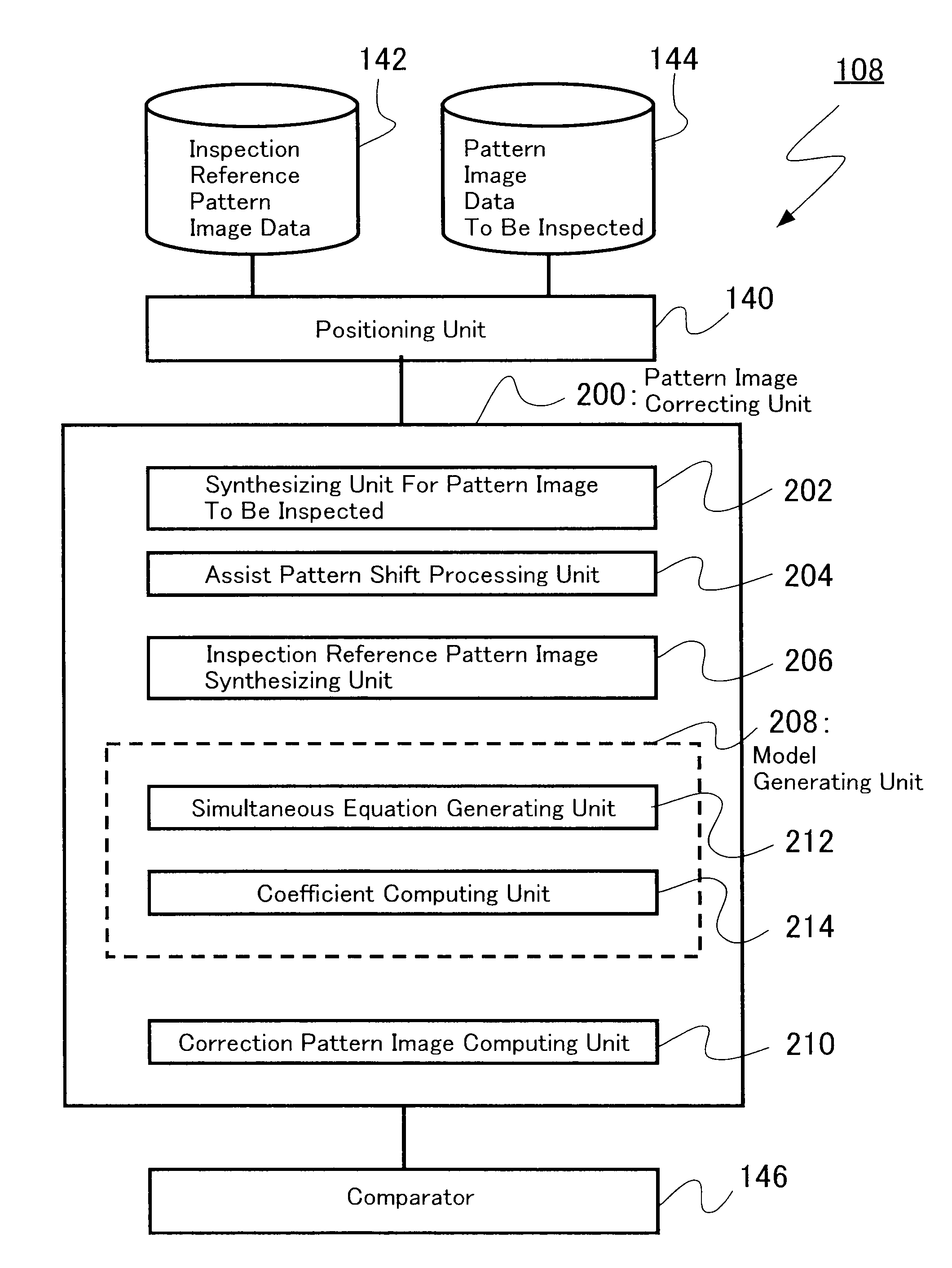
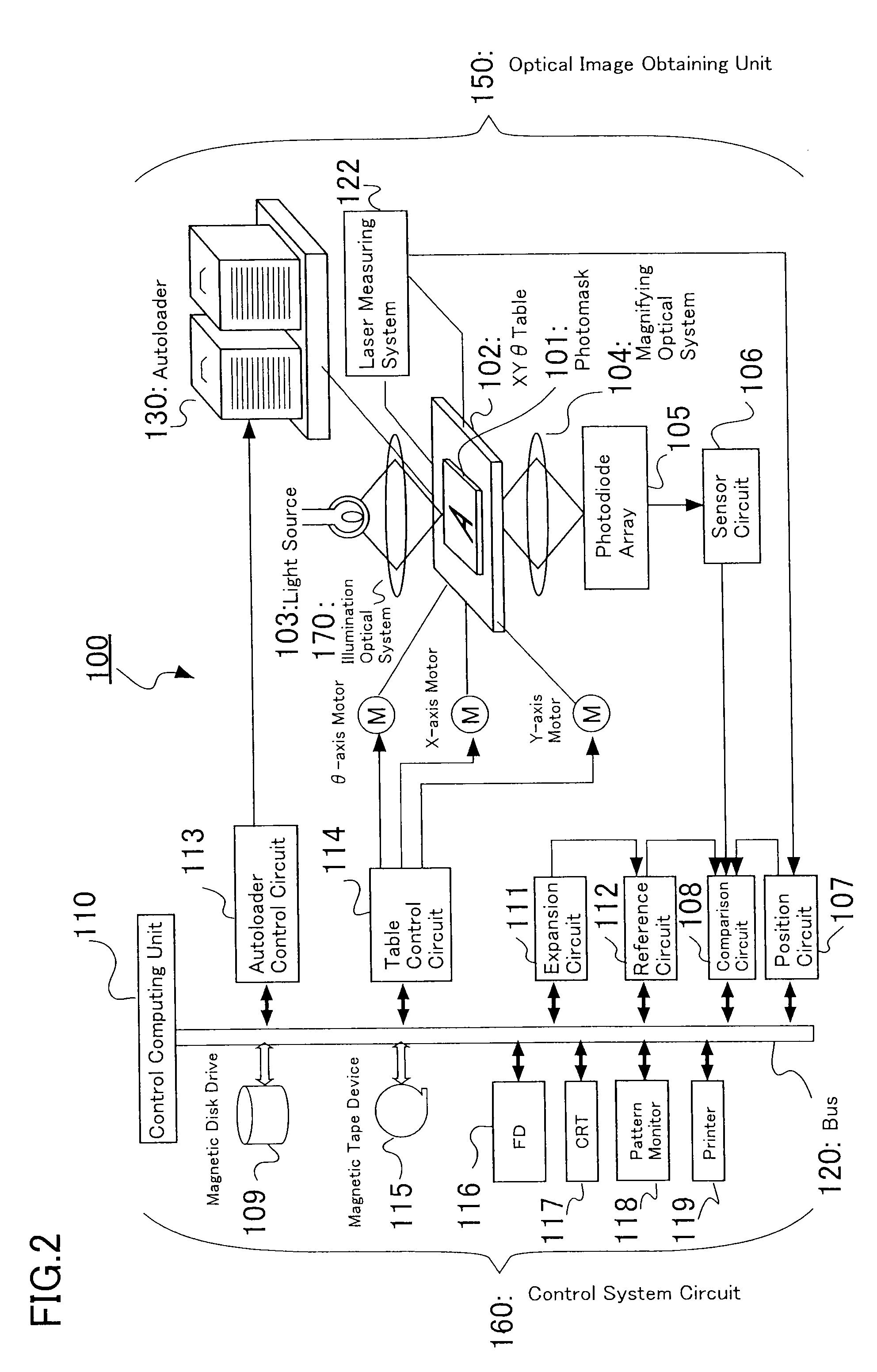
[0025]FIG. 2 is a block diagram showing the configuration of a pattern inspection apparatus of the first embodiment. In the pattern inspection apparatus of FIG. 2, a substrate such as an mask or a wafer on which a pattern is formed is used as a specimen. A pattern inspection apparatus 100 for inspecting a defect in a specimen has an optical image obtaining unit 150 and a control system circuit 160. The optical image obtaining unit 150 has an XYθ table 102, a light source 103, a magnifying optical system 104, a photodiode array 105, a sensor circuit 106, a laser measuring system 122, an auto loader 130, and an illumination optical system 170. In the control system circuit 160, a control computing unit 110 as a computer is connected to a position circuit 107, a comparison circuit 108, an expansion circuit 111, a reference circuit 112, an auto loader control circuit 113, a table control circuit 114, a magnetic disk drive 109, a magnetic tape apparatus 115, a flexible disk drive (FD) 11...

second embodiment

[0070]In the first embodiment, only one kind of an assist pattern image is prepared. However, the invention is not limited to the embodiment. In a second embodiment of the present invention, a configuration of determining pattern density of an image to be inspected and, on the basis of the determination result, selecting a proper assist pattern image from a plurality of assist pattern images prepared will be described. The configuration of the pattern inspection apparatus 100 of the embodiment is similar to that of FIG. 2 except for the internal configuration of the comparison circuit 108. Main steps of a pattern image correcting method in the second embodiment are also similar to those of FIG. 4 except for the assist pattern image selecting step. Therefore, description of the configurations and steps similar to those of the first embodiment will not be repeated.

[0071]FIG. 7 is a block diagram showing the internal configuration of a comparison circuit in the second embodiment. In FI...


PUM


Abstract

The present invention provides an apparatus and method for correcting an inspection reference pattern image in order to properly inspect a pattern image of a specimen. The pattern image correcting apparatus is characterized by including: a first pattern synthesizing unit for synthesizing an assist pattern image and a pattern image to be inspected, thereby generating a pattern image to be inspected with an assist pattern; an assist pattern shift processor; a second pattern synthesizing unit for synthesizing the shifted assist pattern image and the inspection reference pattern image, thereby generating an inspection reference pattern image with an assist pattern; a model generating unit for generating a position shift model by using the pattern image to be inspected with the assist pattern and the inspection reference pattern image with the assist pattern; and a correction pattern image computing unit for correcting the inspection reference pattern image.

Description

CROSS-REFERENCE TO RELATED APPLICATION[0001]This application is based upon and claims the benefit of priority from Japanese Patent Application No. 2008-042997, filed on Feb. 25, 2008, the entire contents of which are incorporated herein by reference.FIELD OF THE INVENTION[0002]The present invention relates to a pattern image correcting apparatus, a pattern inspection apparatus, and a pattern image correcting method. For example, the invention relates to a pattern image correcting apparatus, a pattern inspection apparatus, and a pattern image correcting method applied to an inspection for a defect in a mask for semiconductor lithography.BACKGROUND OF THE INVENTION[0003]In recent years, as a large scale integrated circuit (LSI) is having higher integration and larger capacity, circuit line width required for semiconductor devices is becoming smaller and smaller. The semiconductor devices are manufactured by forming circuits by exposing and transferring a pattern on a wafer by a reduce...

Claims


Application Information

Patent Timeline
Patent Type & Authority Patents(United States)
IPC IPC(8): G06K9/00
CPCG03F1/84G06T7/001G06T2207/10061G06T2207/30148
Inventor SUGIHARA, SHINJI
Owner KIOXIA CORP
Why Eureka
Try Eureka