Film formation method and apparatus for forming silicon-containing insulating film doped with metal

a technology of insulating film and film formation method, which is applied in the direction of liquid surface applicators, semiconductor devices, coatings, etc., can solve the problems of insufficient improvement of electrical characteristics of metal-doped films, difficult to set metal concentrations to be relatively low, etc., and achieve high controllability and relatively low metal concentrations

Inactive Publication Date: 2011-10-11
TOKYO ELECTRON LTD
View PDF6 Cites 64 Cited by
  • Summary
  • Abstract
  • Description
  • Claims
  • Application Information

AI Technical Summary

Benefits of technology

[0009]An object of the present invention is to provide a film formation method and apparatus for a semiconductor process for forming a silicon-containing insulating film doped with a metal, which can set the metal concentration to be relatively lower with high controllability.

Problems solved by technology

However, conventional methods described above for forming a metal-doped film tend to cause the metal concentration to be relatively higher, and thus entails a difficultly in setting the metal concentration to be relatively lower with high controllability.
In this case, the electrical characteristic of the metal-doped film cannot be sufficiently improved.

Method used


Image

  • Film formation method and apparatus for forming silicon-containing insulating film doped with metal
  • Film formation method and apparatus for forming silicon-containing insulating film doped with metal
  • Film formation method and apparatus for forming silicon-containing insulating film doped with metal

Examples


Embodiment Construction

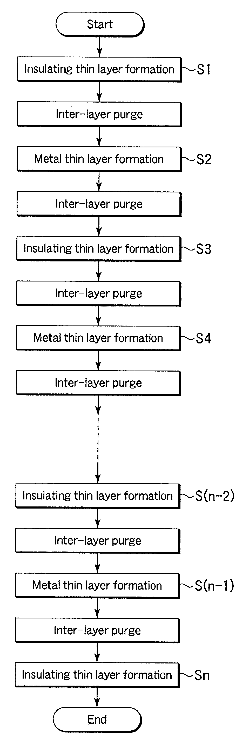
[0023]Embodiments of the present invention will now be described with reference to the accompanying drawings. In the following description, the constituent elements having substantially the same function and arrangement are denoted by the same reference numerals, and a repetitive description will be made only when necessary.

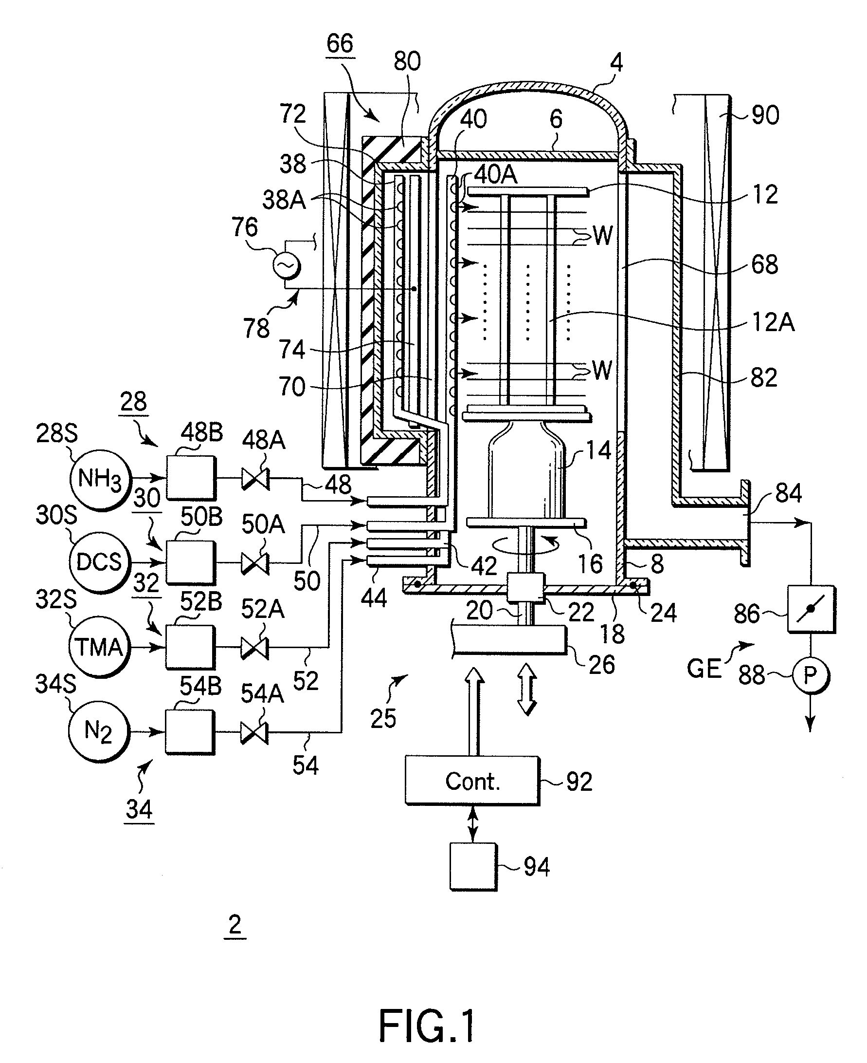
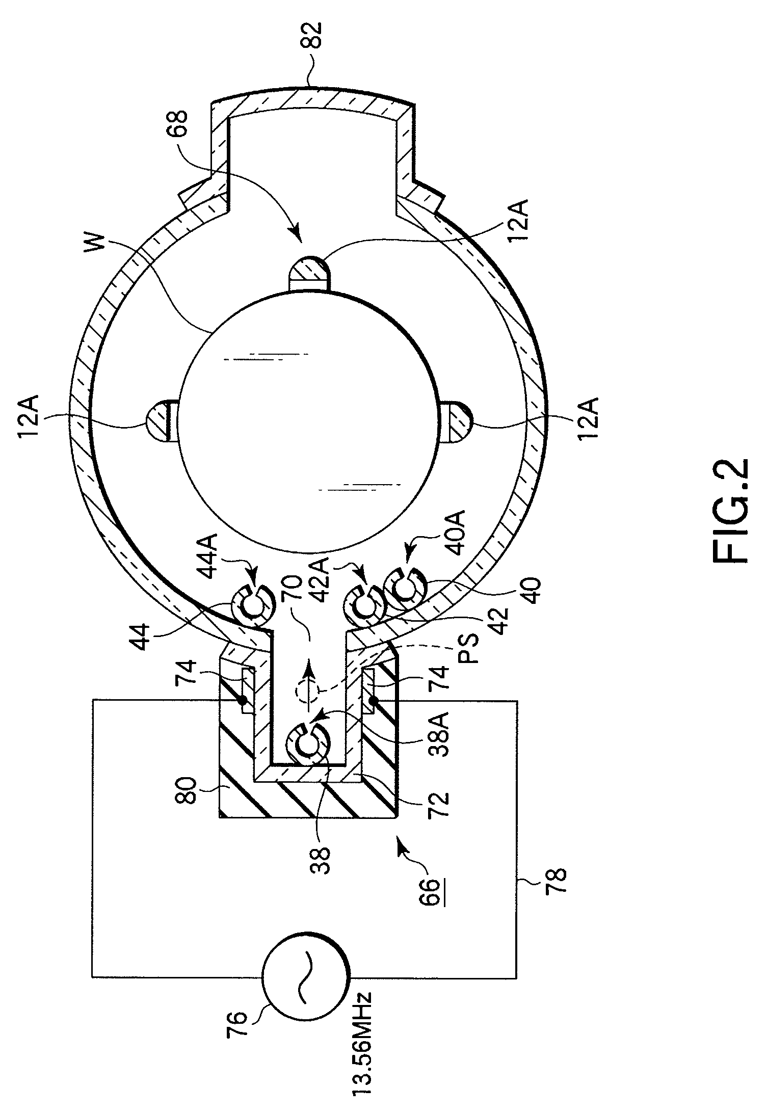
[0024]FIG. 1 is a sectional view showing a film formation apparatus (vertical CVD apparatus) according to an embodiment of the present invention. FIG. 2 is a sectional plan view showing part of the apparatus shown in FIG. 1. The film formation apparatus 2 has a process field configured to be selectively supplied with a first process gas containing dichloro silane (DCS) gas as a silicon source gas, a second process gas containing ammonia (NH3) gas as a nitriding gas or a reducing gas, and a third process gas containing TMA (trimethyl aluminum: organometal compound) gas as a metal source gas. The film formation apparatus 2 is configured to form a silicon nitride fi...


PUM

PropertyMeasurementUnit
thicknessaaaaaaaaaa
thicknessaaaaaaaaaa
thicknessaaaaaaaaaa

Abstract

A film formation method for a semiconductor process performs a film formation process to form a silicon-containing insulating film doped with a metal on a target substrate, in a process field inside a process container configured to be selectively supplied with a silicon source gas and a metal source gas. The method includes forming a first insulating thin layer by use of a chemical reaction of the silicon source gas, while maintaining a shut-off state of supply of the metal source gas; then, forming a first metal thin layer by use of a chemical reaction of the metal source gas, while maintaining a shut-off state of supply of the silicon source gas; and then, forming a second insulating thin layer by use of the chemical reaction of the silicon source gas, while maintaining a shut-off state of supply of the metal source gas.

Description

BACKGROUND OF THE INVENTION[0001]1. Field of the Invention[0002]The present invention relates to a film formation method and apparatus for a semiconductor process for forming a silicon-containing insulating film doped with a metal on a target substrate, such as a semiconductor wafer. The term “semiconductor process” used herein includes various kinds of processes which are performed to manufacture a semiconductor device or a structure having wiring layers, electrodes, and the like to be connected to a semiconductor device, on a target substrate, such as a semiconductor wafer or a glass substrate used for an FPD (Flat Panel Display), e.g., an LCD (Liquid Crystal Display), by forming semiconductor layers, insulating layers, and conductive layers in predetermined patterns on the target substrate.[0003]2. Description of the Related Art[0004]In manufacturing semiconductor devices for constituting semiconductor integrated circuits, a target substrate, such as a semiconductor wafer, is sub...

Claims


Application Information

Patent Timeline
Patent Type & Authority Patents(United States)
IPC IPC(8): H01L21/00
CPCH01L21/02145H01L21/02164H01L21/0217H01L21/022H01L21/28282H01L21/31612H01L21/3185H01L21/02274H01L29/792H01L29/40117H01L21/205
Inventor KADONAGA, KENTAROTONEGAWA, YAMATOCHOU, PAO-HWAHASEBE, KAZUHIDESHIBATA, TETSUYA
Owner TOKYO ELECTRON LTD
Why Eureka
Try Eureka