Method for synthesizing ultrahigh-purity silicon carbide

a technology of polycrystalline silicon carbide and crystal growth method, which is applied in the direction of carbides, cellulosic plastic layered products, natural mineral layered products, etc., can solve the problems of reducing device performance, reducing the electrical properties of the substrate, and reducing the optimum purity of the material for sic semiconductor crystal growth. , to achieve the effect of improving the probability of crystal growth defects, and reducing the number of steps

Inactive Publication Date: 2009-09-03
II VI
View PDF11 Cites 35 Cited by
  • Summary
  • Abstract
  • Description
  • Claims
  • Application Information

AI Technical Summary

Benefits of technology

[0031]The invention is a method of creating so-called “ultrahigh-purity” (UHP) SiC to distinguish this material from other SiC source material previously reported. UHP SiC created in accordance with the present invention exhibits improved crystalline form, chemical stoichiometry, and a high-purity level so that it overcomes several key limitations of the current SiC synthesis methods. The method employs high-purity Si and carbon reactants, specially purified graphite reactor parts, and a high vacuum, rather than an inert gas ambient, during the SiC synthesis. The high vacuum eliminates the major sources of N contamination, such as growth system leaks, N contamination in the inert gas, N absorbed on the graphite insulation and chamber wall, and also reduces other elemental impurities, such as, Cl, S, Al, etc. The resulting product contains concentrations of electrically-active B, Al, and N well below those reported for any other synthesis process, and very low metal concentrations. Test crystals grown from this SiC source are free of polytypism, inclusions and have low micropipe defect densities. The resistivity of the semi-insulating crystals grown from UHP SiC created in accordance with the present invention is above 109 ohm-cm.

Problems solved by technology

Resistivity uniformity of ±10% across a substrate is desired but not often achieved.
Those skilled in SiC crystal growth and devices recognize that the elimination of defects, which degrade device performance, has been a major challenge of the technology development.
None of these methods has yet produced material of optimum purity for SiC semiconductor crystal growth.
SiC produced this way contains hundreds of parts per million (ppm) of impurities, especially electrically-active boron, nitrogen, and aluminum, and in its massed form the SiC is difficult and expensive to separate into particles sized for crystal growth.
Both features make the Acheson prepared material unsuitable as a source material for growth of semiconductor-quality SiC crystals.
Although CVD SiC has been used as a source material for crystal growth, its purity and form are drawbacks to high-yield crystal production.
Typical CVD SiC contains 0.7-2 ppm of boron and up to 100 ppm of nitrogen impurities, which adversely affect crystal growth and make it technically difficult to produce semi-insulating SiC by compensation in order to manufacture microwave devices.
The solid form means source material for each crystal production run must be laboriously cut to fit the growth reactor leading to increased manufacturing costs.
The reactants in this approach often contain extra undesirable and deleterious chemical species such as water, sulfur, nitrogen and oxygen, or involve the introduction of such unwanted species (for example catalysts) as steps in the complicated reaction process.
To reduce such impurities, halogen gases are added during reaction, thus increasing the cost and complexity of the method for making SiC powder.
Additionally, a “constant stream” of non-oxidizing gas is needed to carry away impurities and by-products, adding further technological complexity and cost.
However, in the past, it has proven difficult to obtain the exceptionally high-purity levels, the favored polytype and a particle size optimal for the growth of semiconductor-quality SiC crystals when synthesizing SiC this way.
The resulting product has excessively fine particles of beta polytype.
These properties are poorly matched to the requirements for crystal growth.
In addition, the low purity of the product and its contamination by oxygen would make crystals grown using it as a source unsuitable for semiconductor applications.
Those knowledgeable in the art of SiC synthesis recognize that in this process the C source (lignite or anthracite) is impure, that SiC stoichiometry is difficult to achieve by allowing uncontrolled-Si evaporation, that the process temperatures and moderate vacuum are insufficient to remove N contaminants (indicated by the green color of the resultant product), that in the preferred embodiments the beta polytype is formed, and that the furnace design makes scaling powder production to high volume difficult.
These characteristics make the described process unsuitable for the economic production of SiC crystal growth source material.
The low process temperature, need for a specialized form / size of C particle and the limited size of the batch that can be prepared limit the degree of N removal and lead to high processing costs.
Each of these processes produces a material which contains excessive concentrations of electrically-active shallow dopants, inert elements (mostly metals), or deep level dopants, or which is in a form which increases the probability of crystal growth defects, which adversely affects the electrical properties and uniformity, and reduces the yield of usable substrate material.

Method used


Image

  • Method for synthesizing ultrahigh-purity silicon carbide
  • Method for synthesizing ultrahigh-purity silicon carbide

Examples


example 1

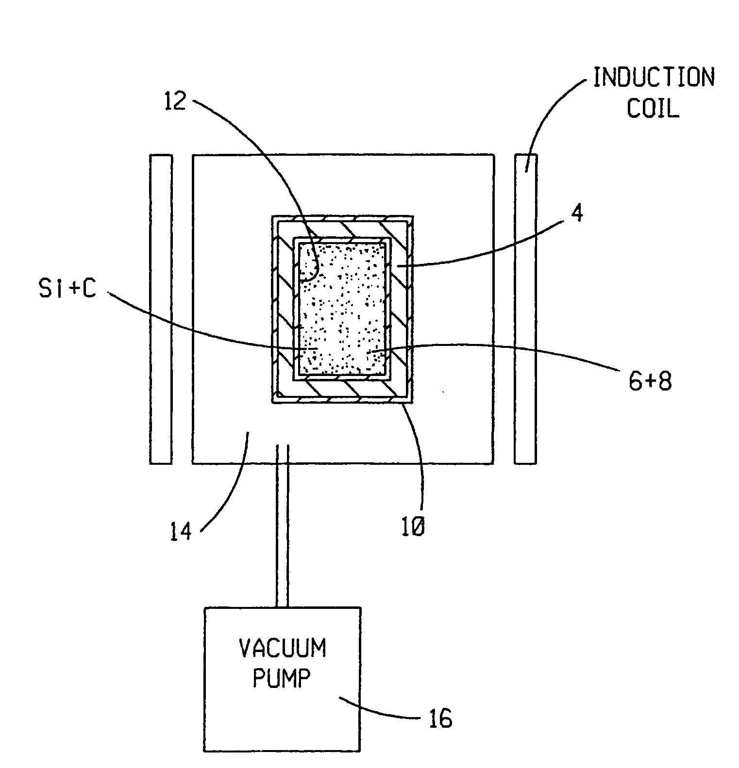
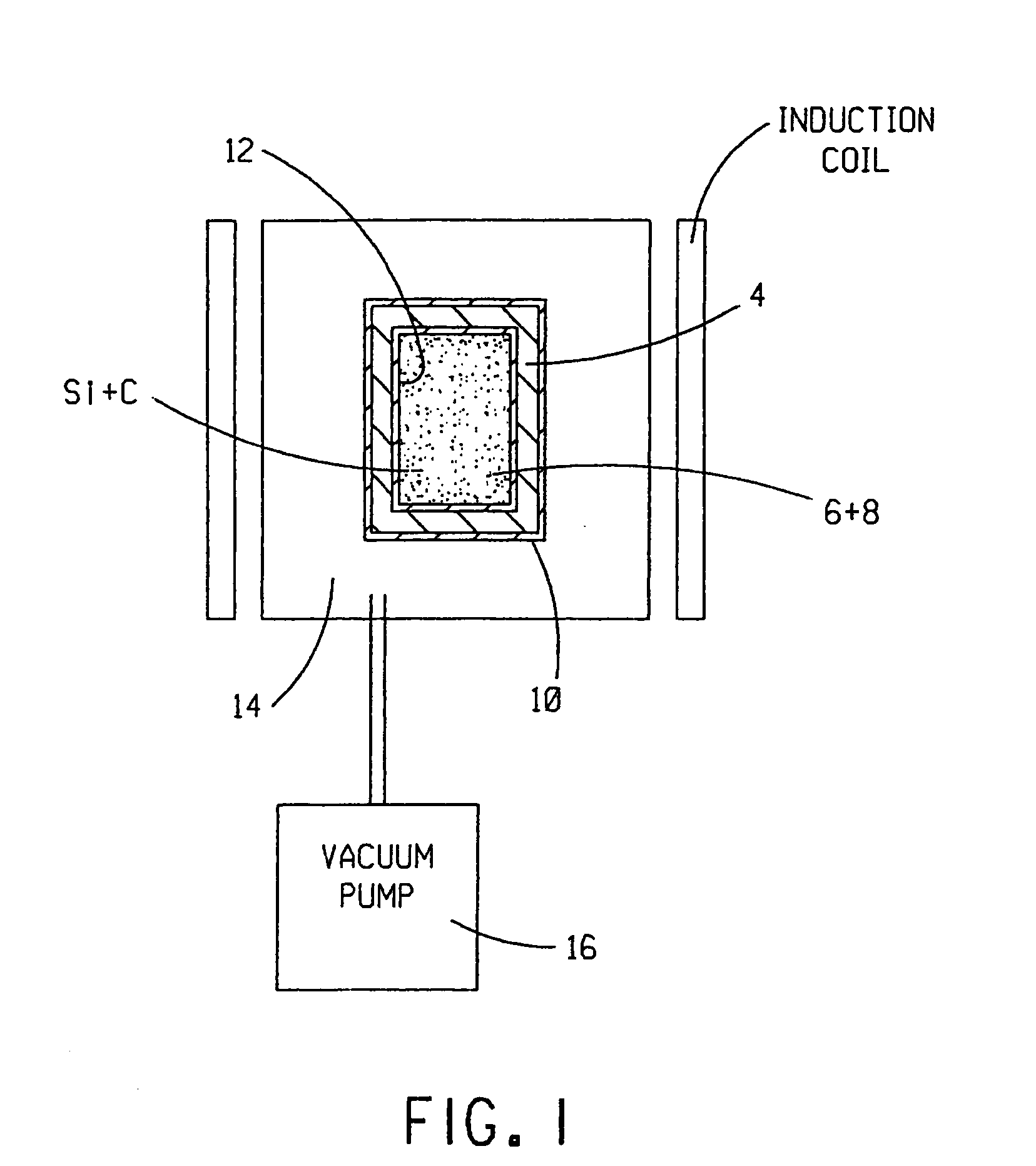
[0053]In an exemplary, non-limiting implementation of the invention, high-purity carbon (C) black powder and semiconductor grade silicon (Si) powder or granules are chosen for the starting materials. Non-limiting examples of suitable high-purity C black powders include THERMAX® and THERMAX ULTRA-PURE® carbon black, both available from Cancarb Limited Corporation, P.O. Box 310, Medicine Hat, Alberta Canada T1A7G1. In the U.S., THERMAX® and THERMAX ULTRA-PURE® are registered trademarks of Cancarb Limited Corporation, U.S. Trademark registration numbers 1,561,698 and 1,526,307, respectively.

[0054]The crucible 4 is formed from high-purity graphite, such as, without limitation, Grade SiC-6 Isotropic Graphite available from Toyo Tanso USA, Inc. of 2575 NW Graham Circle, Troutdale, Oreg. 97060. In one exemplary, non-limiting embodiment, the crucible 4 has an outer diameter of 6 inches, a height of 9 inches, a wall thickness of 0.5 inch and a threaded graphite cap (not shown) configured to ...


PUM

PropertyMeasurementUnit
vacuum pressureaaaaaaaaaa
temperatureaaaaaaaaaa

Abstract

Adsorbed gaseous species and elements in a carbon (C) powder and a graphite crucible are reduced by way of a vacuum and an elevated temperature sufficient to cause reduction. A wall and at least one end of an interior of the crucible is lined with C powder purified in the above manner. An Si+C mixture is formed with C powder purified in the above manner and Si powder or granules. The lined crucible is charged with the Si+C mixture. Adsorbed gaseous species and elements are reduced from the Si+C mixture and the crucible by way of a vacuum and an elevated temperature that is sufficient to cause reduction but which does not exceed the melting point of Si. Thereafter, by way of a vacuum and an elevated temperature, the Si+C mixture is caused to react and form polycrystalline SiC.

Description

BACKGROUND OF THE INVENTION[0001]1. Field of the Invention[0002]The present invention relates to synthesizing polycrystalline ultrahigh-purity (UHP) SiC material useful for growing SiC single crystals to fabricate semiconductor devices for high frequency, high power, high temperature and opto-electronic applications.[0003]2. Description of Related Art[0004]SiC is a semiconductor material that exhibits a unique combination of electrical, chemical and thermo-physical properties that make it extremely attractive and useful for fabricating electronic devices. These properties, which include, without limitation, high breakdown field strength, high operating temperature, good electronic mobility and high thermal conductivity, make possible device operation at significantly higher power, higher temperature and with more resistance to ionizing radiation than comparable devices made from the more conventional semiconductor materials silicon (Si) and GaAs. It has been estimated that transisto...

Claims


Application Information

Patent Timeline
Patent Type & Authority Applications(United States)
IPC IPC(8): C01B31/36B32B5/16
CPCC01B31/36C04B35/573C04B2235/422Y10T428/2982C04B2235/6562C04B2235/6565C04B2235/6584C04B2235/428C01B32/956C01B32/984
Inventor BARRETT, DONOVAN L.CHEN, JIHONGHOPKINS, RICHARD H.JOHNSON, CARL J.
Owner II VI
Why Eureka
Try Eureka