Spacer shape engineering for void-free gap-filling process

a technology of spacer shape and gap-filling process, which is applied in the direction of semiconductor devices, basic electric elements, electrical equipment, etc., can solve the problems of constant effort in scaling of vlsi circuits, circuits becoming smaller and faster, and the distance between devices decreasing, so as to improve the effect of gap-filling

Active Publication Date: 2011-11-01
TAIWAN SEMICON MFG CO LTD
View PDF31 Cites 9 Cited by
  • Summary
  • Abstract
  • Description
  • Claims
  • Application Information

AI Technical Summary

Benefits of technology

In accordance with one aspect of the present invention, a method of forming a semiconductor device includes providing a semiconductor substrate; forming a gate stack on the semiconductor substrate; forming a gate spacer adjacent to a sidewall of the gate stack; thinning the gate spacer; and forming a secondary gate spacer on a sidewall of the gate spacer after the step of thinning the gate spacer.
The advantageous features of the present invention include improved gap-filling, particularly for small-scale integrated circuits.

Problems solved by technology

The scaling of VLSI circuits is a constant effort.
With circuits becoming smaller and faster, however, the distance between devices decreases.
The gap-filling between neighboring devices thus suffers from problems.

Method used


Image

  • Spacer shape engineering for void-free gap-filling process
  • Spacer shape engineering for void-free gap-filling process
  • Spacer shape engineering for void-free gap-filling process

Examples


Embodiment Construction

The making and using of the presently preferred embodiments are discussed in detail below. It should be appreciated, however, that the present invention provides many applicable inventive concepts that can be embodied in a wide variety of specific contexts. The specific embodiments discussed are merely illustrative of specific ways to make and use the invention, and do not limit the scope of the invention.

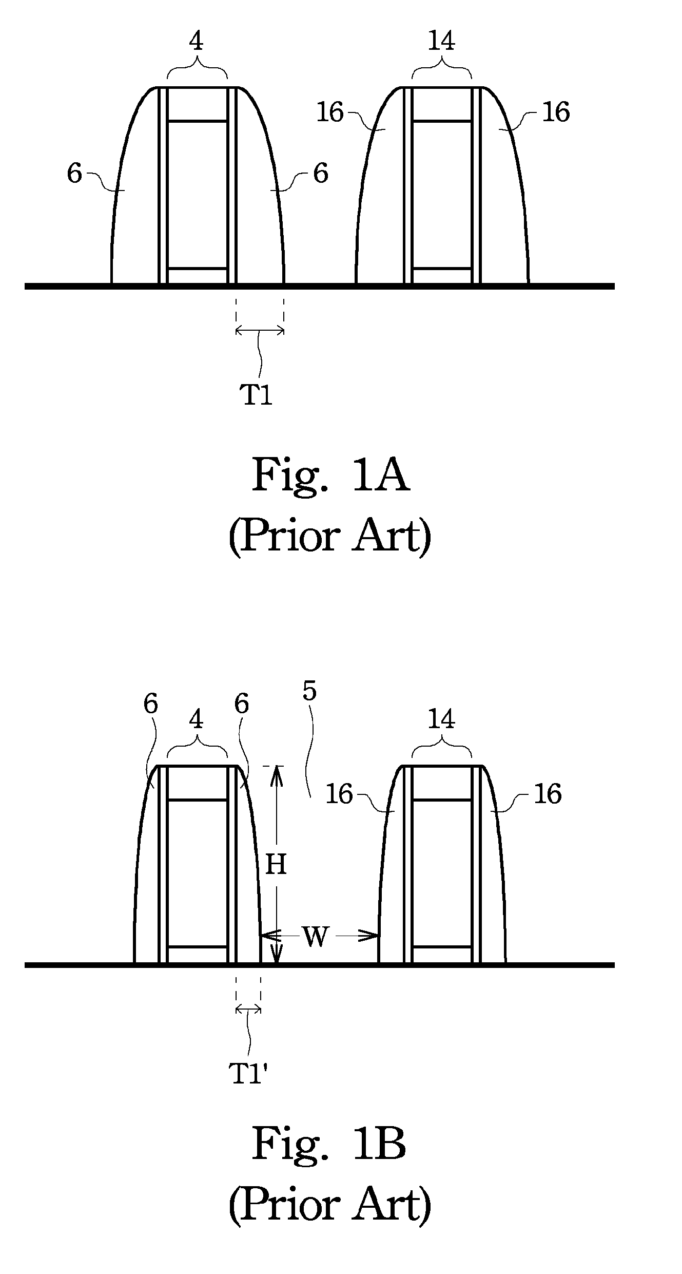
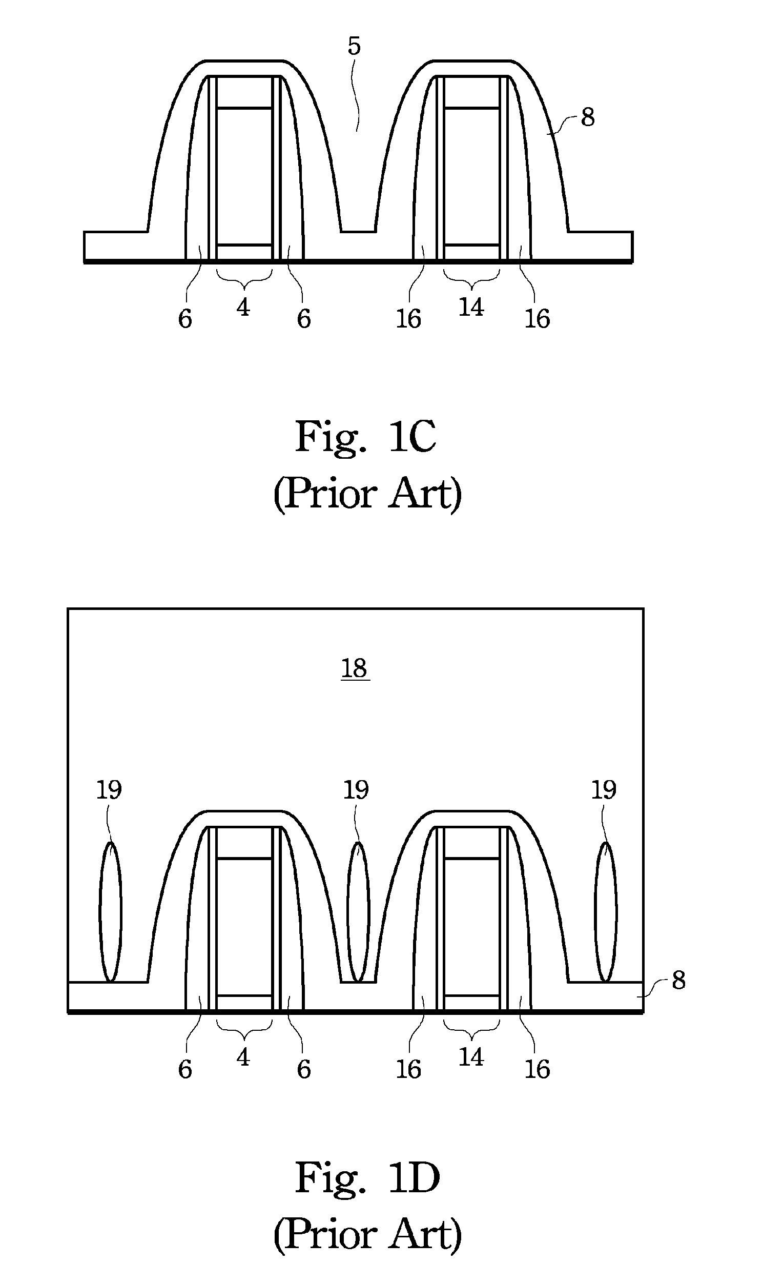
A novel method for forming metal-oxide-semiconductor devices and filling the gaps therebetween is provided. The intermediate stages of manufacturing a preferred embodiment of the present invention are illustrated. The variations of the preferred embodiments are then discussed. Throughout the various views and illustrative embodiments of the present invention, like reference numbers are used to designate like elements.

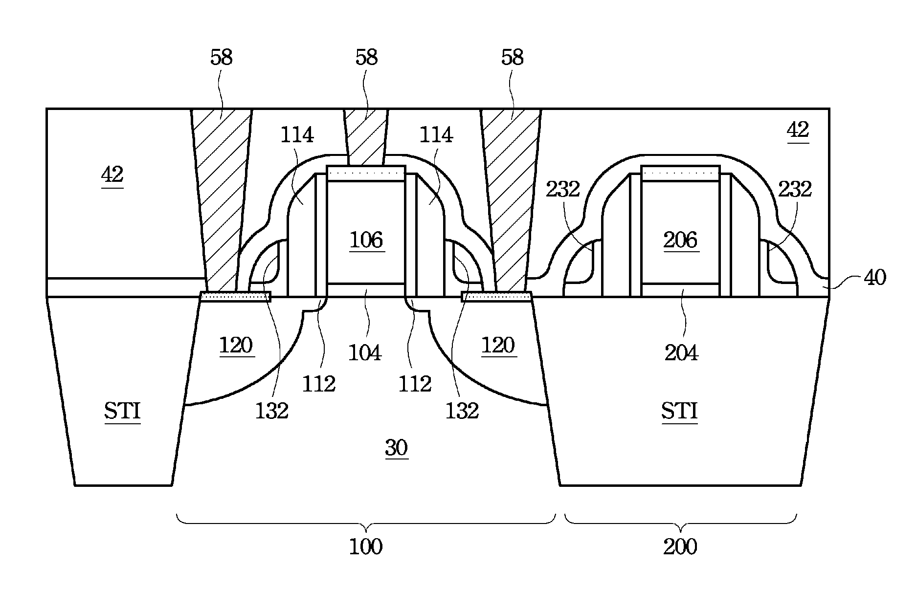
Referring to FIG. 2, substrate 30 is provided. Substrate 30 includes regions 100 and 200 adjacent to each other. In an embodiment, region 100 is for forming a MOS devi...


PUM


Abstract

A method of forming a semiconductor device includes providing a semiconductor substrate; forming a gate stack on the semiconductor substrate; forming a gate spacer adjacent to a sidewall of the gate stack; thinning the gate spacer; and forming a secondary gate spacer on a sidewall of the gate spacer after the step of thinning the gate spacer.

Description

TECHNICAL FIELDThis invention relates generally to semiconductor devices, and more particularly to structures and manufacturing methods of metal-oxide-semiconductor (MOS) devices with improved gap-filling.BACKGROUNDThe scaling of VLSI circuits is a constant effort. Smaller integrated circuits allow more devices to be formed in one semiconductor chip. Additionally, power consumption and performance are also improved. With circuits becoming smaller and faster, however, the distance between devices decreases. The gap-filling between neighboring devices thus suffers from problems. The gap-filling problem may be explained using FIGS. 1A through 1D. Referring to FIG. 1A, gate stacks 4 and 14 are formed close to each other. Gate spacers 6 and 16 are formed on sidewalls of gate stacks 4 and 14, respectively. Referring to FIG. 1B, gate spacers 6 and 16 are thinned, so that their thickness T1 as shown in FIG. 1A is reduced to thickness T1′ as in FIG. 1B. In FIG. 1C, contact etch stop layer (C...

Claims


Application Information

Patent Timeline
Patent Type & Authority Patents(United States)
IPC IPC(8): H01L21/336
CPCH01L21/823468H01L21/823475H01L21/823481H01L29/6653H01L29/6656H01L29/7833H01L29/7843
Inventor WU, MING-YUANMOR, YI-SHIENPENG, CHIH-TANGYEH, CHIUNG-HANTHEI, KONG-BENGCHUANG, HARRYLIANG, MONG-SONG
Owner TAIWAN SEMICON MFG CO LTD
Why Eureka
Try Eureka