Spin-on-dielectric process

a spin-on dielectric and dielectric technology, applied in the direction of coatings, liquid surface applicators, electrical devices, etc., can solve the problems of voids in films transformed by dielectric materials, becomes a challenge to eliminate voids, etc., to improve the gap filling capability of flowable materials, reduce viscos and increase fluidity of flowable materials

Inactive Publication Date: 2018-12-20
UNITED MICROELECTRONICS CORP +1
View PDF4 Cites 0 Cited by
  • Summary
  • Abstract
  • Description
  • Claims
  • Application Information

AI Technical Summary

Benefits of technology

[0006]According to the above, the present invention provides a spin-on-dielectric process, which heats a flowable material while spread it on a surface of a substrate, especially for heating the flowable material to a temperature higher than 25° C., to form a spin-on-dielectric layer on the substrate. By doing this, the viscosity of the flowable material is reduced, the fluidity of the flowable material is increased and the gap filling capability of the flowable material is improved. Hence, voids in the formed spin-on-dielectric layer can be avoided.

Problems solved by technology

However, voids may occur in the films transformed by the dielectric material, which usually occurs at the bottom of the trenches.
Thus, it becomes a challenge to eliminate the voids in the films.

Method used


Image

  • Spin-on-dielectric process
  • Spin-on-dielectric process
  • Spin-on-dielectric process

Examples


Embodiment Construction

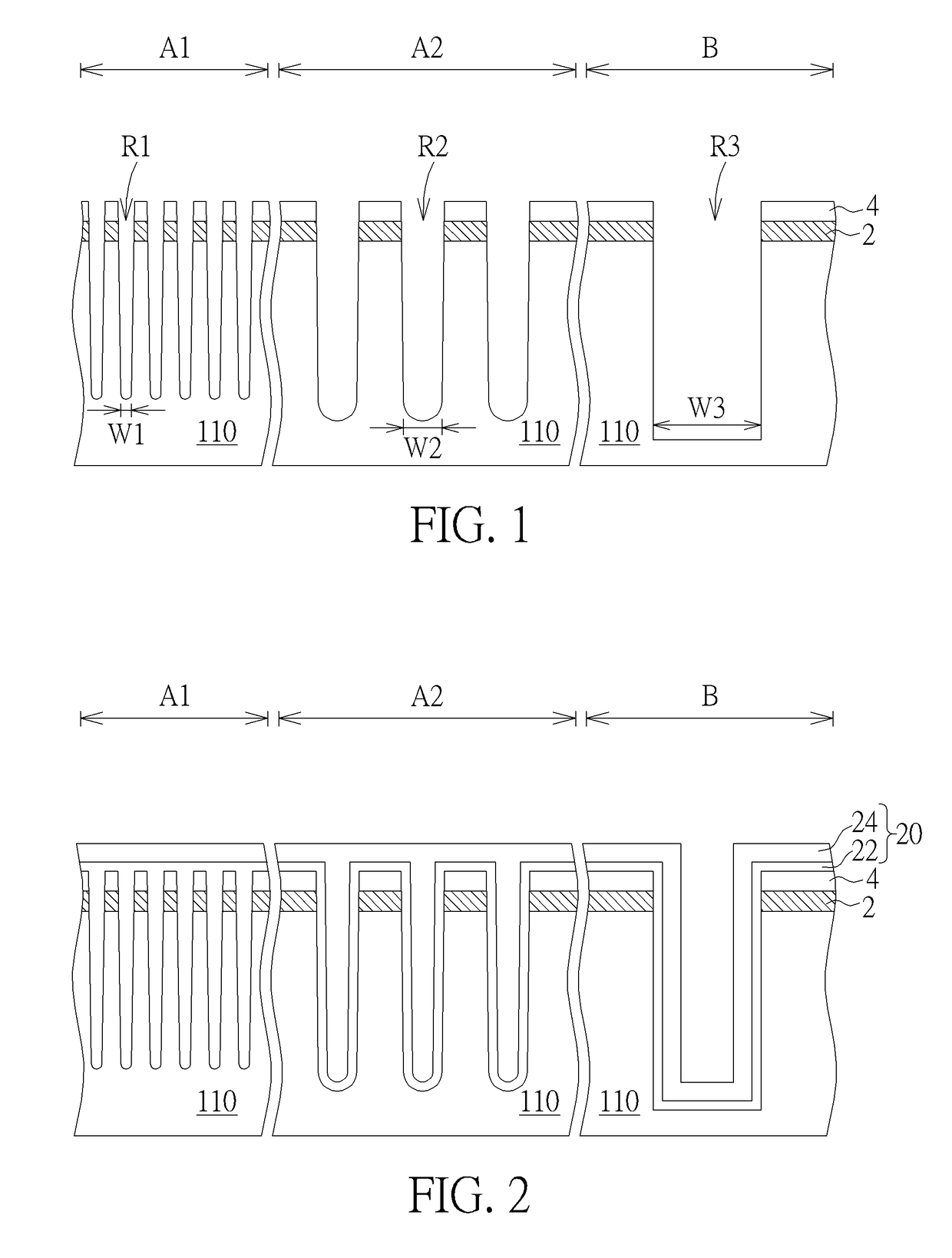
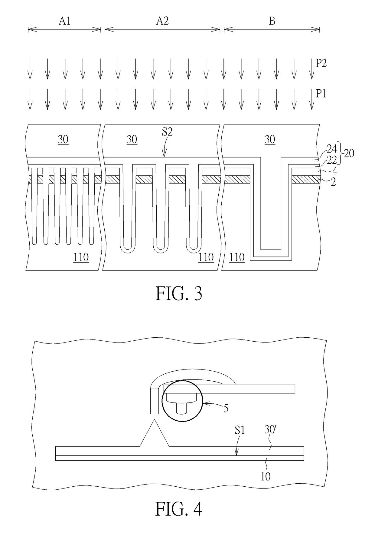
[0017]FIGS. 1-3 schematically depict cross-sectional views of an improved spin-on-dielectric process according to an embodiment of the present invention. As shown in FIG. 1, a substrate 110 is provided. The substrate 110 may be a semiconductor substrate such as a silicon substrate, a silicon containing substrate, a III-V group-on-silicon (such as GaN-on-silicon) substrate, a graphene-on-silicon substrate or a silicon-on-insulator (SOI) substrate. The substrate 110 may be divided into a first area A1, a second area A2 and a third area B. For instance, the first area A1 and the second area A2 may be memory cell areas while the third area B may be a peripheral area, wherein circuits in the peripheral area are used to operate memory cells in the memory cell areas, but it is not limited thereto. In this embodiment, a plurality of memory cells are disposed in each of the memory cell areas, to forma dynamic random access memory (DRAM) device having recessed gate structures, but it is not l...


PUM

PropertyMeasurementUnit
temperatureaaaaaaaaaa
viscosityaaaaaaaaaa

Abstract

A spin-on-dielectric process includes the following steps. A substrate is provided. A flowable material is spread on a surface of the substrate to forma spin-on-dielectric layer on the substrate, wherein the flowable material is heated to a temperature higher than 25° C.

Description

BACKGROUND OF THE INVENTION1. Field of the Invention[0001]The present invention relates generally to a coating process, and more specifically to a spin-on-dielectric (SOD) process.2. Description of the Prior Art[0002]Dielectric materials are often deposited by spin-on dielectric (SOD) process or chemical vapor deposition (CVD) process. While using the spin-on dielectric (SOD) process, a flowable dielectric material can be coated into gaps in a substrate easily through adjusting dibasic ester (DBE) system. This is an unique advantage of the spin-on dielectric (SOD) process, and thus the spin-on dielectric (SOD) process is widely used in nowadays industry.[0003]Trenches with different sizes are usually formed in a substrate. A dielectric material covers the surface of the trenches while coating the dielectric material on the substrate by the spin-on dielectric (SOD) process. However, voids may occur in the films transformed by the dielectric material, which usually occurs at the botto...

Claims


Application Information

Patent Timeline
Patent Type & Authority Applications(United States)
IPC IPC(8): B05D1/00B05C11/08H01L21/02H01L21/762
CPCB05D1/005B05C11/08H01L21/02282H01L21/76224H01L21/76229H01L21/02222
Inventor LEE, JUI-MINCHANG, CHING-HSIANGHUANG, CHENG-HSUCHEN, YI-WEILIU, WEI-HSINTZOU, SHIH-FANG
Owner UNITED MICROELECTRONICS CORP
Why Eureka
Try Eureka