Methods for improving low k FSG film gap-fill characteristics

a film and gap-filling technology, applied in the field of integrated circuit manufacturing, can solve the problems of increasing the aspect ratio gap in some applications, and the difficulty of filling spaces using conventional methods, and achieve the effect of improving the gap-filling characteristics

Inactive Publication Date: 2008-06-24
APPLIED MATERIALS INC
View PDF13 Cites 2 Cited by
  • Summary
  • Abstract
  • Description
  • Claims
  • Application Information

AI Technical Summary

Benefits of technology

[0007]To address these and other needs, the present invention provides, in part, fluorinated silicon oxide films with low dielectric constants and improved gap-fill characteristics.
[0010]In another aspect of the invention, a method of improving the gap-fill characteristics of a low k fluorine-containing silicon oxide film is provided. The method generally comprises: (a) providing a gas mixture comprising a fluorinated silicon source, a fluorine source different from said fluorinated silicon source, a hydrogen source, and a oxidizer to a high density plasma chemical vapor deposition (HDP-CVD) chamber for deposition of a low k fluorine-containing silicon oxide film on a substrate via high density plasma chemical vapor deposition (HDP-CVD); and (b) generating a plasma within said HDP-CVD chamber to thereby deposit said low k fluorine-containing silicon oxide film on said substrate; wherein said gas mixture does not comprise a silane compound having the general formula SixHy, wherein x has a range of 1 to 2, y has a range of 4 to 6; and wherein said deposited low k fluorine-containing silicon oxide film exhibits improved gap-fill characteristics, as compared to films deposited without said gas mixture.
[0011]In yet another aspect of the invention, a second method of improving the gap-fill characteristics of a low k fluorine-containing silicon oxide film is provided. This method generally comprises: (a) providing a gas mixture comprising a fluorinated silicon source, a carbon source, a hydrogen source, and a oxidizer to a high density plasma chemical vapor deposition (HDP-CVD) chamber for deposition of a low k fluorine-containing silicon oxide film on a substrate via high density plasma chemical vapor deposition (HDP-CVD); and (b) generating a plasma within said HDP-CVD chamber to thereby deposit said low k fluorine-containing silicon oxide film on said substrate; wherein said gas mixture does not comprise a silane compound having the general formula SixHy, wherein x has a range of 1 to 2, y has a range of 4 to 6; and wherein said deposited low k fluorine-containing silicon oxide film exhibits improved gap-fill characteristics, as compared to films deposited without said gas mixture.

Problems solved by technology

Smaller feature sizes have resulted in the presence of increased aspect ratio gaps for some applications, for example, between adjacent conductive lines or in etched trenches.
These spaces are difficult to fill using conventional methods.

Method used


Image

  • Methods for improving low k FSG film gap-fill characteristics
  • Methods for improving low k FSG film gap-fill characteristics
  • Methods for improving low k FSG film gap-fill characteristics

Examples


Embodiment Construction

I. Introduction

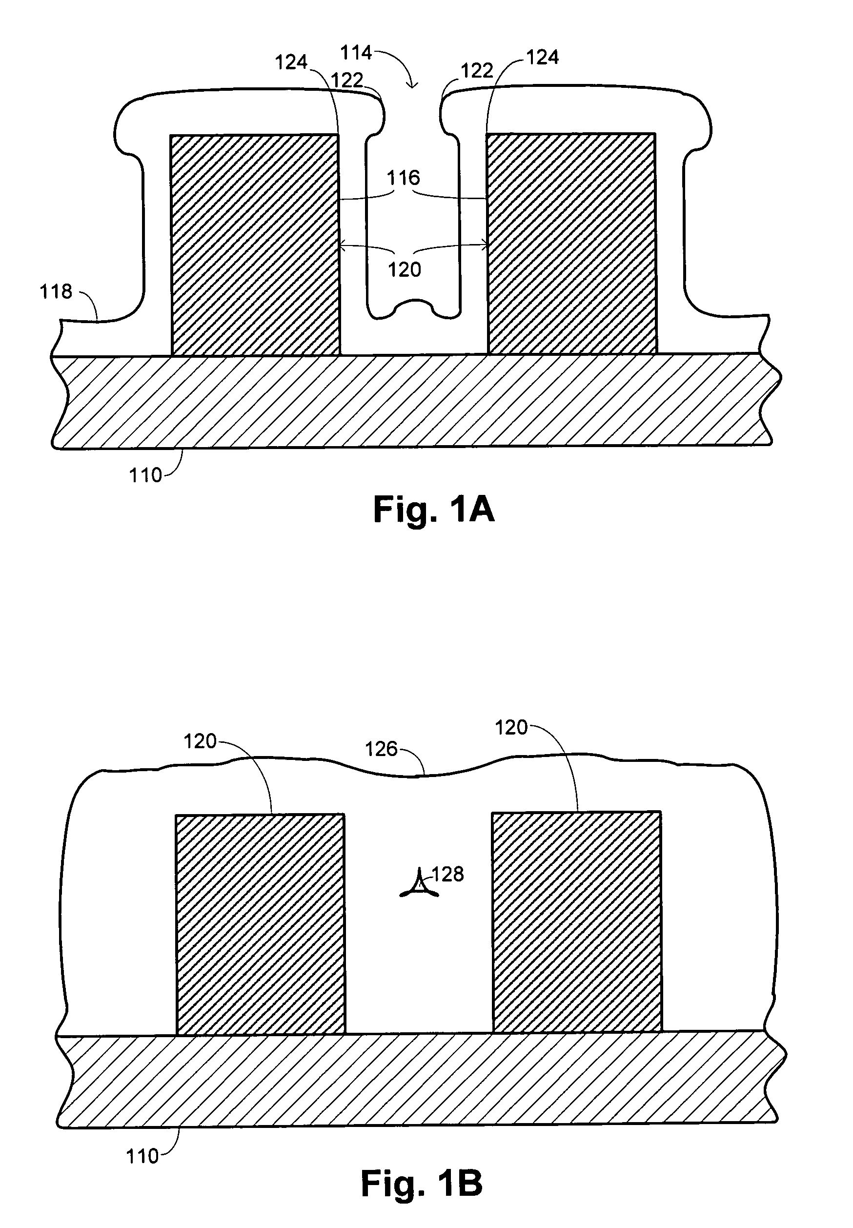
[0018]The gap-fill problem addressed by embodiments of the invention is illustrated schematically with the cross-sectional views shown in FIGS. 1A and 1B. FIG. 1A shows a vertical cross section of a substrate 110, such as may be provided with a semiconductor wafer, having a layer of features 120. Adjacent features define gaps 114 that are to be filled with dielectric material 118, with the sidewalls 116 of the gaps being defined by the surfaces of the features 120. As the deposition proceeds, dielectric material 118 accumulates on the surfaces of the features 120, as well as on the substrate 110 and forms overhangs 122 at the corners 124 of the features 120. As deposition of the dielectric material 118 continues, the overhangs 122 typically grow faster than the gap 114 in a characteristic bread-loafing fashion. Eventually, the overhangs 122 grow together to form the dielectric layer 126 shown in FIG. 1B, preventing deposition into an interior void 128.

[0019]CVD deposi...


PUM

PropertyMeasurementUnit
temperatureaaaaaaaaaa
pressureaaaaaaaaaa
dielectric constantaaaaaaaaaa

Abstract

The present invention relates to fluorinated silicate glass (FSG) with low dielectric constant and improved gap-fill characteristics. In the present method, a fluorinated silicon source, an optional fluorine source, an optional carbon source, a hydrogen source, and an oxygenator are used as the reactant gases. Inert or carrier gas(es) may also be used. In accordance with the present invention, the reactant gas mixture does not comprise a silane compound having the general formula SixHy, wherein x has a range of 1 to 2, y has a range of 4 to 6. The material deposited is thus referred to herein alternatively as “SixFy-only FSG” or “SixFy-only fluorinated oxide” (“SOFO”).

Description

BACKGROUND OF THE INVENTION[0001]The present invention relates to the manufacture of integrated circuits, and more specifically, to methods, apparatus and systems for forming fluorinated silicate glass (“FSG”) films with improved characteristics in a high-density-plasma chemical-vapor-deposition (“HDP-CVD”) environment.[0002]Semiconductor device geometries have dramatically decreased in size since such devices were first introduced several decades ago. Smaller feature sizes have resulted in the presence of increased aspect ratio gaps for some applications, for example, between adjacent conductive lines or in etched trenches. The aspect ratio of a gap is defined by the ratio of the gap's height or depth to its width. These spaces are difficult to fill using conventional methods. A film's ability to completely fill such gaps is referred to as the film's “gap-filling” ability. Silicon oxide is one type of insulation film that is commonly used to fill the gaps in intermetal dielectric (...

Claims


Application Information

Patent Timeline
Patent Type & Authority Patents(United States)
IPC IPC(8): H01L21/31
CPCC23C16/045C23C16/401H01J37/321H01L21/02131H01L21/02211H01L21/02274H01L21/31629H01L21/76837
Inventor WOO, SEONG-OHCHOI, JUN TAE
Owner APPLIED MATERIALS INC
Why Eureka
Try Eureka