
Preparation method of STI (shallow trench isolation) structure

An isolation structure and shallow trench technology, which is applied in semiconductor/solid-state device manufacturing, electrical components, circuits, etc., can solve problems affecting film shrinkage and gap healing, shallow trench isolation technology is difficult to reconcile, and active silicon loss, etc. Achieve the effects of full filling, smooth groove, and diffusion prevention

Inactive Publication Date: 2014-01-22
SHANGHAI HUALI MICROELECTRONICS CORP
View PDF6 Cites 9 Cited by
  • Summary
  • Abstract
  • Description
  • Claims
  • Application Information

AI Technical Summary

Problems solved by technology

[0012] 5) Annealing: In this step, in the annealing process of traditional shallow groove isolation preparation, wet annealing is adopted, and steam is introduced, and the steam generates oxidation active hydroxide (-OH) at high temperature, and hydroxide (-OH) is easy Penetrate the silicon dioxide layer 110 / 130 to oxidize the active silicon in the semiconductor substrate 100 to generate silicon dioxide: 2H 2 O+Si→SiO 2 +2H 2 , resulting in the loss of silicon in the semiconductor substrate 100
However, steam at high temperature produces oxidatively active hydroxide (-OH), which easily penetrates the silicon dioxide layer (SiO 2 ) to oxidize active silicon, i.e. steam annealing will result in loss of active silicon
Avoiding or alleviating this problem can be achieved by lowering the temperature of steam annealing or reducing the annealing time, but at the same time, it will affect the shrinkage of the film and the healing of the gap filled by the high aspect ratio process, which has become a contradiction that is difficult to reconcile in the existing shallow trench isolation technology question

Method used


Image

  • Preparation method of STI (shallow trench isolation) structure
  • Preparation method of STI (shallow trench isolation) structure
  • Preparation method of STI (shallow trench isolation) structure

Examples


Embodiment Construction

[0033] In order to make the purpose, technical solution and advantages of the present invention clearer, the following will further describe the implementation of the present invention in detail in conjunction with the accompanying drawings.

[0034] Those skilled in the art can easily understand other advantages and effects of the present invention from the contents disclosed in this specification. The present invention can also be implemented or applied through other different specific implementation modes, and various modifications or changes can be made to the details in this specification based on different viewpoints and applications without departing from the spirit of the present invention.

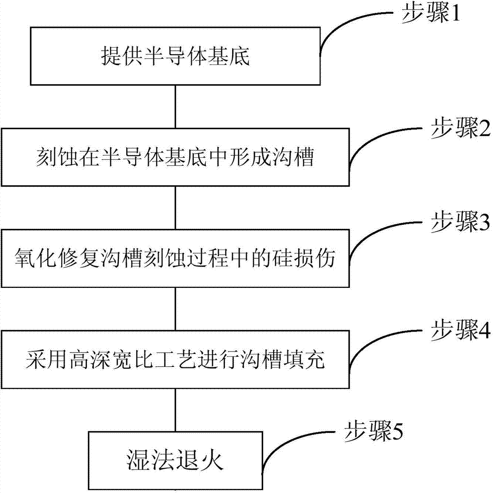
[0035] image 3 It is a flow chart of the steps of the preparation method of the shallow trench isolation structure provided by the present invention.

[0036] like image 3 As shown, the method for preparing a shallow trench isolation structure provided in this specific embodim...


PUM


Abstract

The invention relates to the technical field of semiconductors and discloses a preparation method of an STI structure. The preparation method comprises the steps as follows: providing a semiconductor substrate covered with a silicon dioxide layer on the surface; forming a trench in the semiconductor substrate by etching; forming a silicon dioxide film covering the surface of the trench by oxidizing the bottom and side walls of the trench; forming a linear silicon nitride layer on the structure surface of the trench; forming a linear silicon dioxide layer on the surface of the linear silicon nitride layer; depositing a silicon dioxide filling layer and filling the trench; and annealing. Compared with the prior art, the preparation method has the advantages that the compact and stable silicon dioxide layer is introduced, so that the diffusion of water vapor or oxygen molecules can be stopped, and the silicon loss caused by high-temperature wet annealing is effectively prevented; and meanwhile, the annealing temperature can also be increased due to introduction of the silicon nitride layer, so that filling gaps in a high aspect ratio process can be improved, and the high-quality STI structure can be obtained.

Description

technical field [0001] The invention relates to the field of semiconductor technology, in particular to a method for preparing a shallow trench isolation structure in a semiconductor process. Background technique [0002] With the rapid development of semiconductor technology, the feature size of semiconductor devices has been significantly reduced, and correspondingly higher requirements have been put forward for the chip manufacturing process. One of the challenging issues is the uniform and non-porous filling of insulating dielectric between various thin film layers or in trenches to provide sufficient and effective isolation protection. [0003] After the manufacturing process entered the deep submicron technology node, the improved LOCOS structure had serious bird's beak effect and field oxygen thinning effect, so shallow trench isolation (STI) technology appeared. The formation of the shallow trench isolation structure first needs to be in Grooves are etched in the su...

Claims


Application Information

Patent Timeline
Patent Type & Authority Applications(China)
IPC IPC(8): H01L21/762
CPCH01L21/76224
Inventor 江润峰戴树刚
Owner SHANGHAI HUALI MICROELECTRONICS CORP
Learn More