Semiconductor component and method for fabricating the same

a technology of semiconductors and components, applied in the direction of semiconductor devices, semiconductor/solid-state device details, electrical equipment, etc., can solve the problems of difficult to achieve the desired depth of etching in the trench, and the need to overcom

Inactive Publication Date: 2008-12-04
NAN YA TECH
View PDF4 Cites 0 Cited by
  • Summary
  • Abstract
  • Description
  • Claims
  • Application Information

AI Technical Summary

Benefits of technology

[0016]Accordingly, the present invention is directed to a semiconductor componen...

Problems solved by technology

However, currently there are still some problems that need to be overcome when forming isolation structures...

Method used


Image

  • Semiconductor component and method for fabricating the same
  • Semiconductor component and method for fabricating the same
  • Semiconductor component and method for fabricating the same

Examples


Embodiment Construction

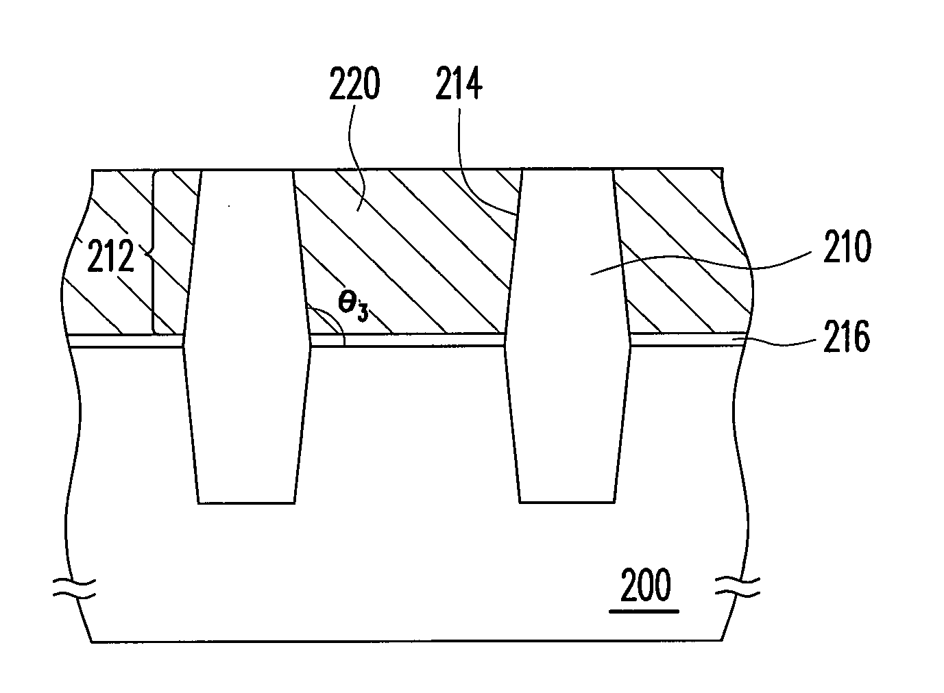
[0043]A floating gate structure is used as an example to illustrate the semiconductor component of the present invention and the method for fabricating the same in the following description.

[0044]FIGS. 2A through 2D are cross-sectional views illustrating a process for fabricating a floating gate structure according to one embodiment of the present invention.

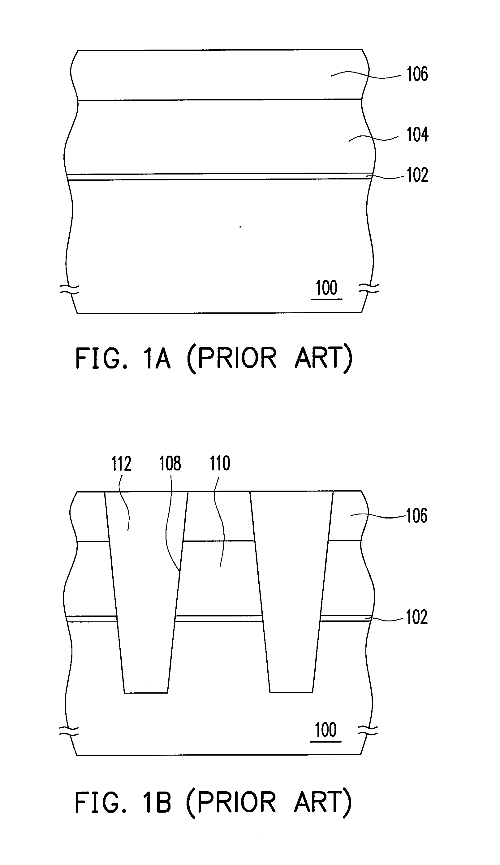
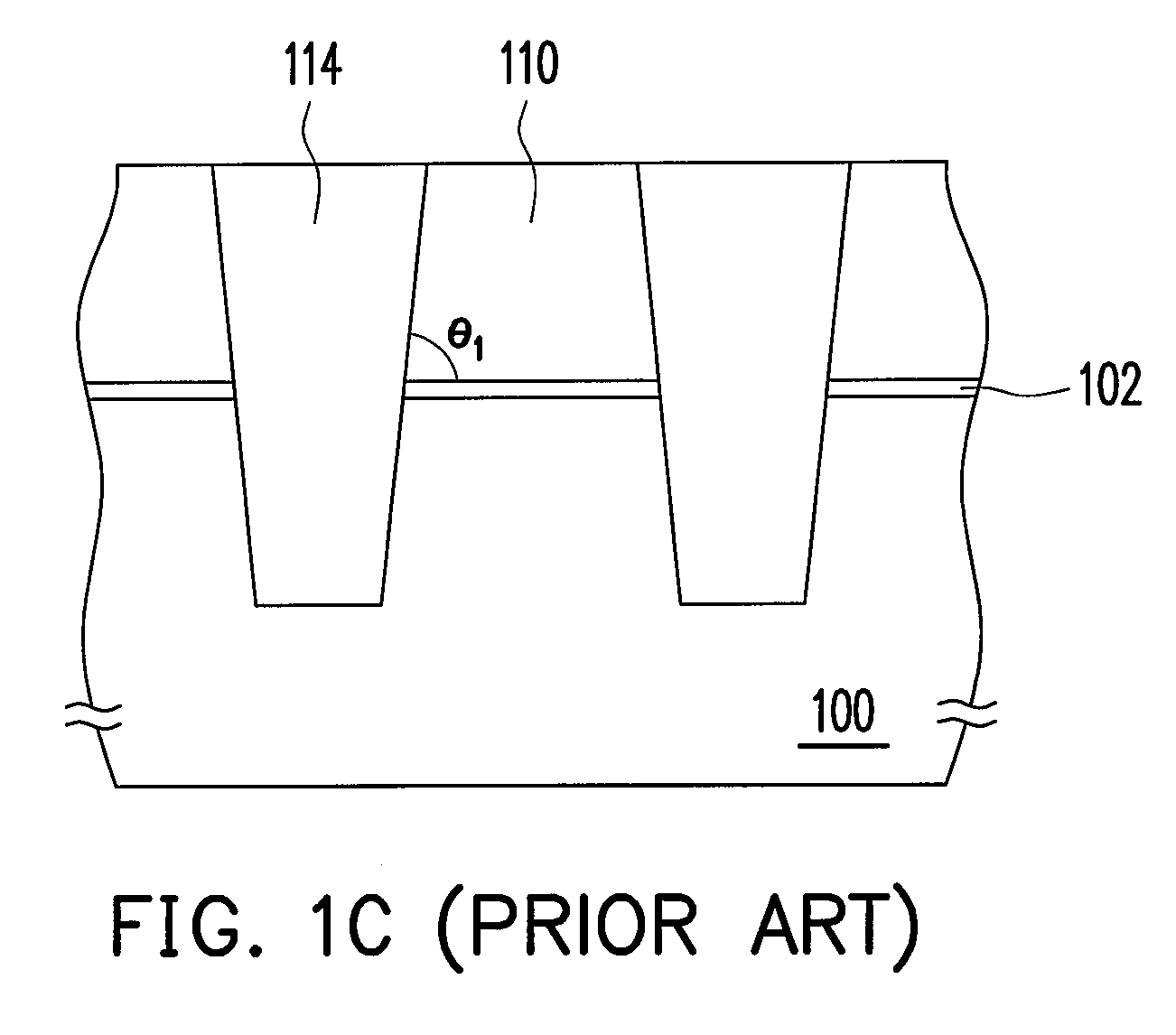
[0045]Referring to FIG. 2A, a mask layer 202 is formed on a substrate 200. The substrate 200 is, for example, a silicon substrate. The material used for fabricating the mask layer 202 is, for example, silicon nitride. The method used for forming the mask layer 202 is, for example, a chemical vapor deposition process.

[0046]Further, prior to the formation of the mask layer 202, a pad oxide layer 204 may be selectively formed on the substrate 200. The pad oxide layer 204 can prevent the generation of stress by the mask layer 202 on the substrate 200 and enhance the adhesion between the mask layer 202 and the substrate 200. The metho...


PUM


Abstract

A semiconductor component includes a substrate, two isolation structures, a conductor pattern and a dielectric layer. The isolation structures are disposed in the substrate, and each of the isolation structures has protruding portions protruding from the surface of the substrate. A trench is formed between the protruding portions. The included angle formed by the sidewall of the protruding portion and the surface of the substrate is an obtuse angle. The conductor pattern is disposed in the trench and fills the trench up. The dielectric layer is disposed between the conductor pattern and the substrate.

Description

CROSS-REFERENCE TO RELATED APPLICATION[0001]This application claims the priority benefit of Taiwan application serial no. 96118909, filed on May 28, 2007. The entirety of the above-mentioned patent application is hereby incorporated by reference herein and made a part of this specification.BACKGROUND OF THE INVENTION[0002]1. Field of the Invention[0003]The present invention relates to a semiconductor component and, more particularly to a semiconductor component and a method for fabricating the same.[0004]2. Description of Related Art[0005]In semiconductor device fabrication process, the quality of isolation structures can have a significant influence on the electrical performance of semiconductor components. However, currently there are still some problems that need to be overcome when forming isolation structures. A floating gate structure that forms a flash memory device is used as an example in the following description.[0006]A flash memory device is a non-volatile memory that al...

Claims


Application Information

Patent Timeline
IPC IPC(8): H01L23/00H01L21/76
CPCH01L21/823481H01L27/11521H10B41/30
Inventor HSIAO, CHING-NANHUANG, CHUNG-LINTSAI, CHEN-YULEE, CHUNG-YUAN
Owner NAN YA TECH
Why Eureka
Try Eureka