Method of forming polycrystalline silicon layer and atomic layer deposition apparatus used for the same
What is AI technical title?
AI technical title is built by PatSnap AI team. It summarizes the technical point description of the patent document.
a technology of atomic layer deposition and polycrystalline silicon, which is applied in the direction of chemical vapor deposition coating, vacuum evaporation coating, coating, etc., can solve the problems of poor interface characteristics between the polycrystallized silicon semiconductor layer and the gate insulating layer, requiring a long processing time, and deformation of the substra
Inactive Publication Date: 2011-11-01
SAMSUNG DISPLAY CO LTD
View PDF60 Cites 364 Cited by
Summary
Abstract
Description
Claims
Application Information
AI Technical Summary
This helps you quickly interpret patents by identifying the three key elements:
Problems solved by technology
Method used
Benefits of technology
Benefits of technology
This approach allows for faster crystallization at lower temperatures, reduces substrate deformation, improves interface characteristics, and enables mass production suitability by controlling seed position and grain size, enhancing the efficiency and cost-effectiveness of polycrystalline silicon layer formation.
Problems solved by technology
However, the SPC method requires a long processing time, and easily causes deformation of a substrate due to long annealing at high temperature, and the ELC method requires high-priced laser equipment and has poor interface characteristics between the polycrystallized silicon semiconductor layer and a gate insulating layer due to protrusions occurring on the polycrystallized surface.
However, in these methods, metal particles to be deposited randomly propagate from a metal target, and thus there is a limit in being able to uniformly deposit a metal catalyst to have a concentration as high as 1011 to 1016 atoms / cm2.
Recently, while a technique of uniformly depositing crystallization-inducing metals on an amorphous silicon layer using micro-electro-mechanical systems (MEMS) technology has been disclosed, this has disadvantages of length of preparation time in mass-production, which may not be suitable for commercialization.
Method used
Image
Click on the blue label to locate the original text in one second.
Reading with bidirectional positioning of images and text.
Examples
Embodiment Construction
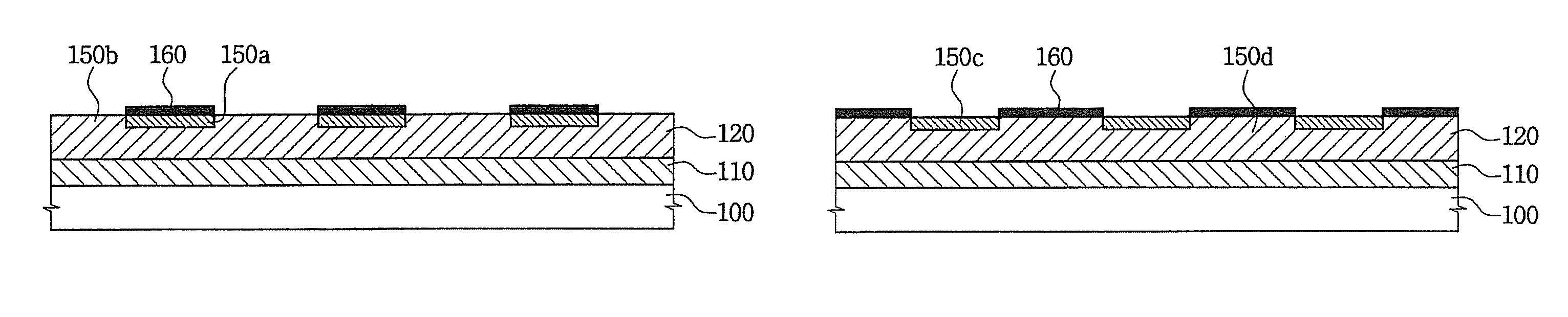
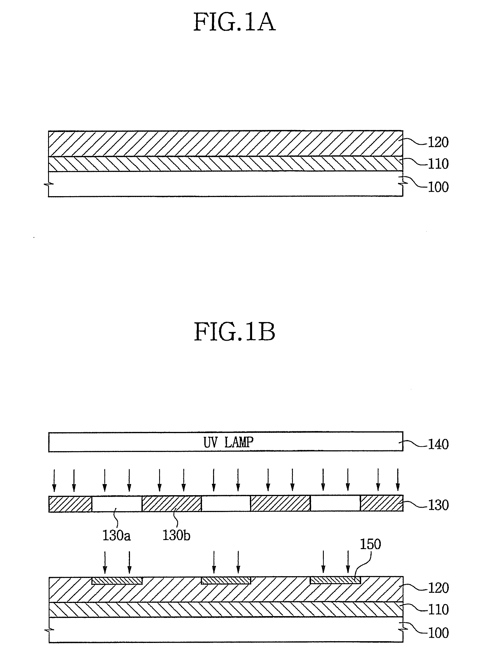
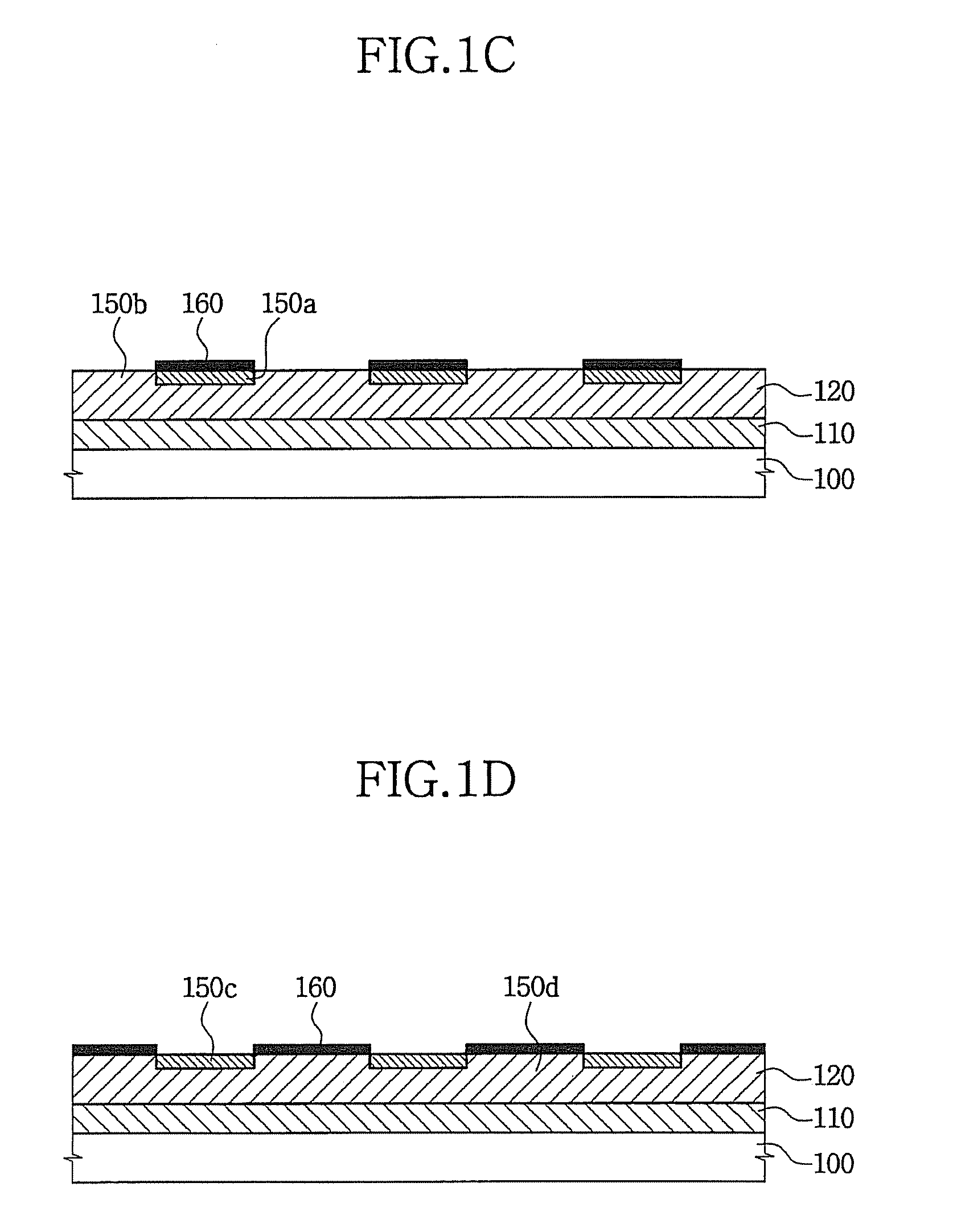
[0017]Reference will now be made in detail to the present embodiments of the present invention, examples of which are illustrated in the accompanying drawings, wherein like reference numerals refer to the like elements throughout. The embodiments are described below in order to explain the present invention by referring to the figures.
[0018]FIGS. 1A to 1D are cross-sectional views illustrating a method of forming a polycrystalline silicon layer according to an exemplary embodiment of the present invention. Referring to FIG. 1A, a substrate 100 formed of glass or plastic is prepared. A buffer layer 110 may be formed on the substrate 100. The buffer layer 110 is formed of a single insulating layer including silicon dioxide or silicon nitride, or a multilayer thereof, by chemical vapor deposition (CVD) or physical vapor deposition (PVD). Here, the buffer layer 110 may prevent diffusion of moisture or impurities generated from the substrate 100, or control the heat transfer rate during ...
CROSS-REFERENCE TO RELATED APPLICATION[0001]This application claims the benefit of Korean Patent Application No. 10-2009-0018927, filed Mar. 5, 2009 in the Korean Intellectual Property Office, the disclosure of which is incorporated herein by reference.BACKGROUND OF THE INVENTION[0002]1. Field of the Invention[0003]Aspects of the present invention relate to a method of forming a polycrystalline silicon layer and an atomic layer deposition apparatus used for the same, and more particularly, to a method of forming a polycrystalline silicon layer and an atomic layer deposition apparatus in which a crystallization-inducing metal may be deposited on an amorphous silicon layer at a predetermined position and a uniform concentration by modifying a predetermined region of a surface of the amorphous silicon layer into a hydrophilic surface or a hydrophobic surface. Thus, seed position and grain size may be controlled.[0004]2. Description of the Related Art[0005]Generally, polycrystalline sil...
Claims
Application Information
Patent Timeline
Application Date:The date an application was filed.
Publication Date:The date a patent or application was officially published.
First Publication Date:The earliest publication date of a patent with the same application number.
Issue Date:Publication date of the patent grant document.
PCT Entry Date:The Entry date of PCT National Phase.
Estimated Expiry Date:The statutory expiry date of a patent right according to the Patent Law, and it is the longest term of protection that the patent right can achieve without the termination of the patent right due to other reasons(Term extension factor has been taken into account ).
Invalid Date:Actual expiry date is based on effective date or publication date of legal transaction data of invalid patent.

