

Semiconductor device
a semiconductor and chip technology, applied in the direction of electrical apparatus contruction details, final product manufacturing, dielectric characteristics, etc., can solve the problems of affecting the electric performance of the semiconductor device, the difference in expansion and contraction between the components, etc., and achieve the effect of reducing the possibility of local undulation
- Summary
- Abstract
- Description
- Claims
- Application Information
AI Technical Summary
Benefits of technology
Problems solved by technology
Method used
Image

Examples
embodiment 1
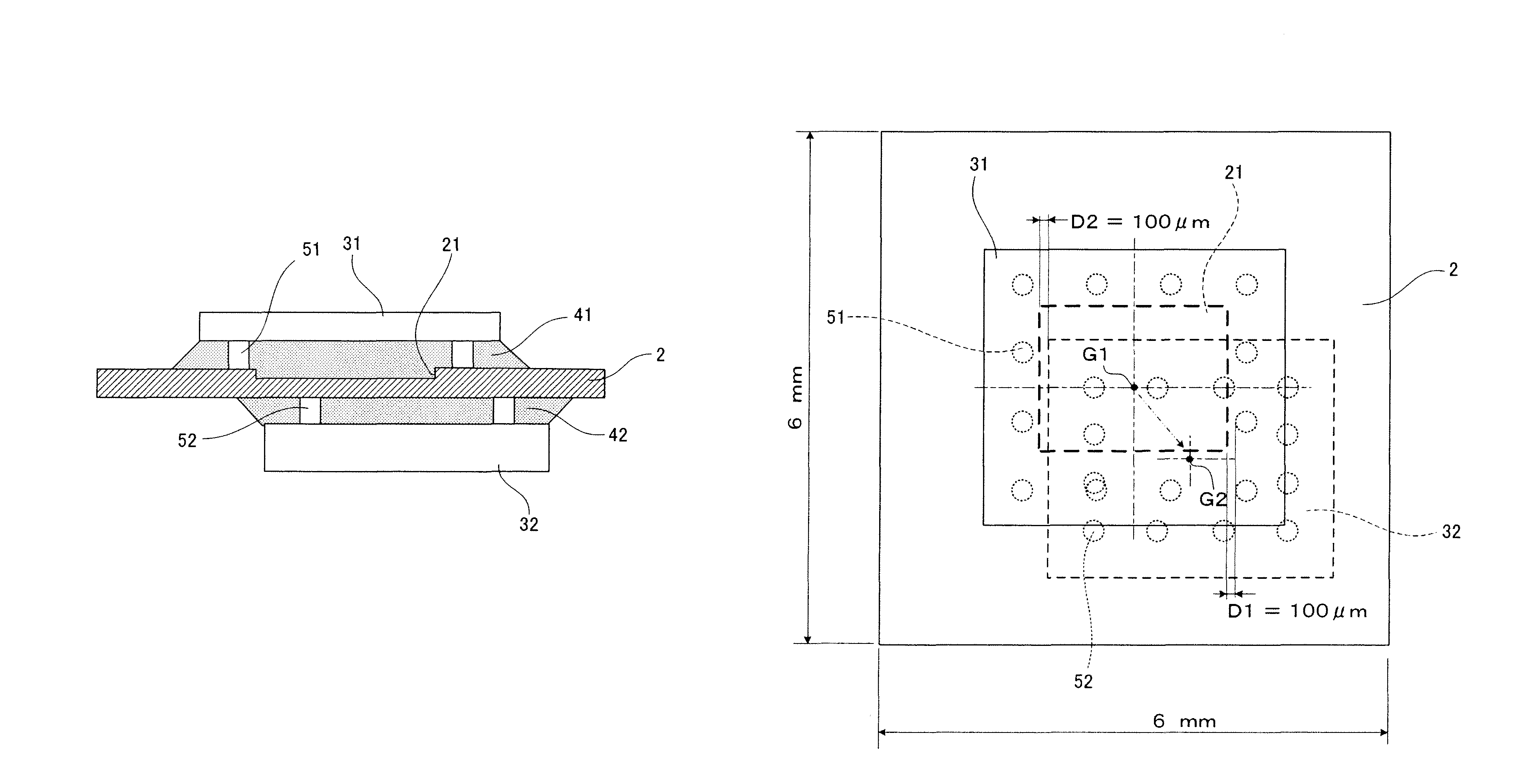
[0033]FIGS. 1A and 1B show Embodiment 1 of the present invention.
[0034]A semiconductor chip 31 is flip-flop mounted face-down on the top surface of a circuit board 2. A semiconductor chip 32 is flip-flop mounted face-down on the bottom surface of the circuit board 2.
[0035]Specifically, a molding adhesive resin 41 is formed on the top surface of the circuit board 2. The semiconductor chip 31 is mounted on the molding adhesive resin 41. The semiconductor chip 31 is externally shaped to have, in this case, a length of 3 mm, a width of 3 mm, and a thickness of 200 μm, which are an example of dimensions in a system LSI.
[0036]The circuit board 2 is externally shaped to have a length of 6 mm, a width of 6 mm, and a thickness of 300 μm. The circuit board 2 is a double-side circuit board with a 6-layer configuration. Although not shown in detail, electrodes on the surface of the circuit board 2 are electrically joined to pads on the surface of the semiconductor chip 31 via bumps 51. The bump...
embodiment 2
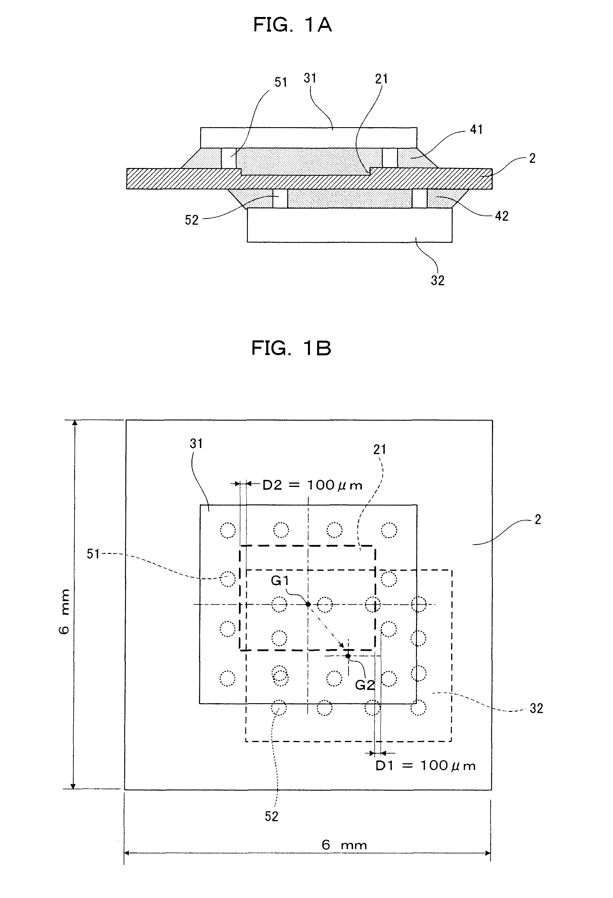
[0049]FIGS. 2 and 3 show Embodiment 2 of the present invention.
[0050]In Embodiment 1, the entire recess portion 21 formed on the top surface of the circuit board 2 is formed in the area in which the semiconductor chips 31 and 32 overlap. However, if it is difficult to form this owing to restrictions on electric wiring on a circuit board 2, then as shown in FIG. 2, a recess portion 21 may be formed restrictively in a key-shaped area along a position corresponding to the outer periphery of a semiconductor chip 32, where a tensile force reaches the maximum. This structure exerts effects similar to those of Embodiment 1. In this case, the width of the key-shaped recess portion 21 is at least 200 μm in total, that is, the sum of at least 100 μm outside the semiconductor chip 32 and at least 100 μm inside the semiconductor chip 32.
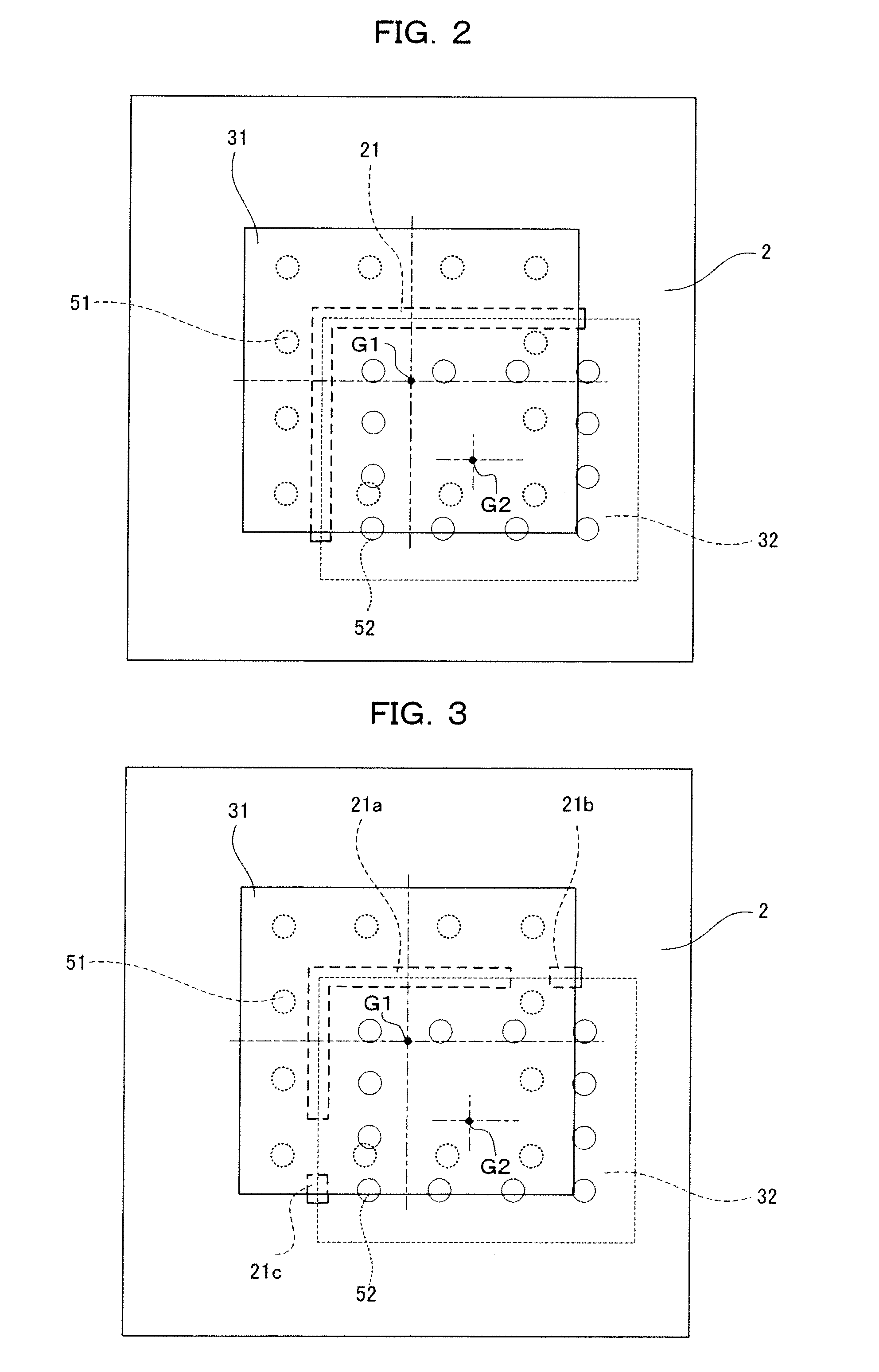
[0051]Furthermore, the square recess portion 21 shown in FIGS. 1A and 1B or the recess portion 21 located in the key-shaped area as shown in FIG. 2 is formed co...
embodiment 3
[0053]FIGS. 4A and 4B show Embodiment 3 of the present invention.
[0054]In Embodiment 3, as shown in FIGS. 4A and 4B, a protruding portion 22 is formed on a surface of a circuit board 2 on which a semiconductor chip 31 is mounted. The protruding portion 22 is about 30 μm in height.
[0055]The protruding portion 22 is composed of any material such as an epoxy resin containing glass cloth with a larger elastic modulus than a molding adhesive resin. Specifically, the molding adhesive resin has an elastic modulus of about 5 GPa. The epoxy resin containing glass cloth has an elastic modulus of at least 10 GPa.
[0056]Such a hard material is formed on the circuit board 2 to locally increase the thickness of the circuit board in the area containing the material. This prevents the semiconductor chip 31 from being affected by the warpage of a semiconductor chip 32 mounted on the opposite side of the circuit board 2. Thus, a possible tensile force exerted on the interface between the semiconductor...
PUM
 Abstract
Description
Claims
Application Information