Patterning method of organic electroluminescent device

a technology of organic electroluminescent and patterning method, which is applied in the direction of sustainable manufacturing/processing, instruments, and final product manufacturing, etc., can solve the problems of insufficient ultraviolet ray irradiation effect, difficult to efficiently perform patterning with high definition, and difficulty in high-definition patterning, etc., to achieve excellent design properties and enhance the productivity of organic el panels

Inactive Publication Date: 2011-11-08
YAMAGATA PROMOTIONAL ORG FOR INDAL TECH
View PDF9 Cites 2 Cited by
  • Summary
  • Abstract
  • Description
  • Claims
  • Application Information

AI Technical Summary

Benefits of technology

[0011]The present invention is accomplished in order to solve the foregoing technical problems, and its object is to provide a patterning method of an organic EL device by irradiation of ultraviolet ray, that can easily and efficiently be performed with high definition, and that can control a contrast by a luminous brightness.

Problems solved by technology

However, these methods entail problems as follows.
In the conventional patterning method, it is difficult to cope with high definition of the pattern.
When ultraviolet ray is irradiated after a panel is formed, transmittance of the ultraviolet ray at a transparent substrate and a transparent electrode is insufficient, so that sufficient effect of the irradiation of ultraviolet ray cannot be obtained.
Therefore, it is difficult to efficiently perform patterning with high definition.
In this patterning method, the area of the EL device where ultraviolet ray is irradiated is made a non-emission area, resulting in that the contrast in the emission area cannot be controlled.

Method used


Image

  • Patterning method of organic electroluminescent device
  • Patterning method of organic electroluminescent device
  • Patterning method of organic electroluminescent device

Examples


example 1

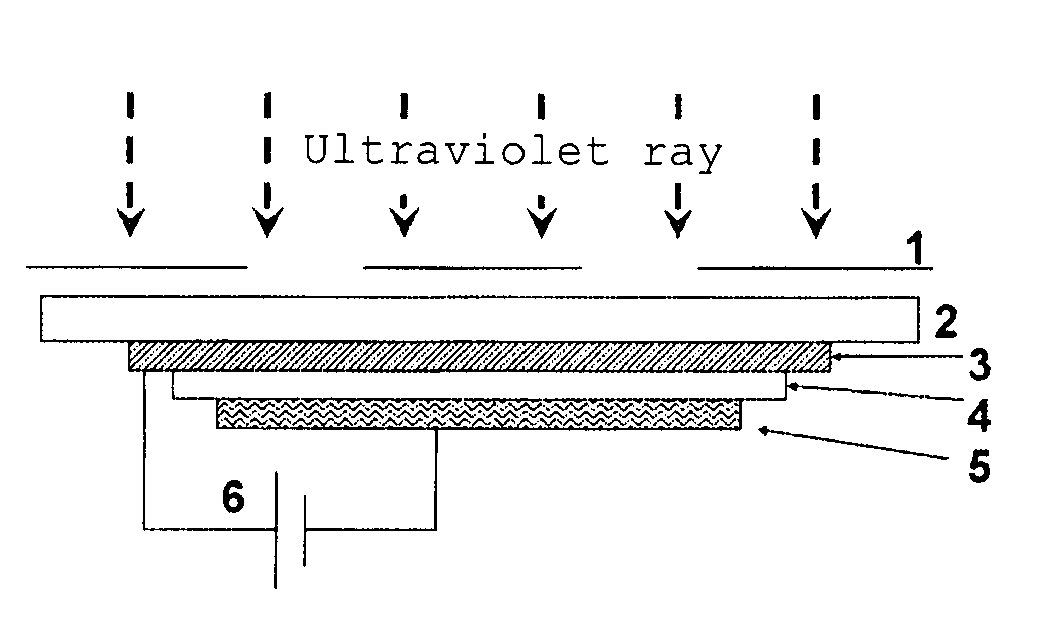
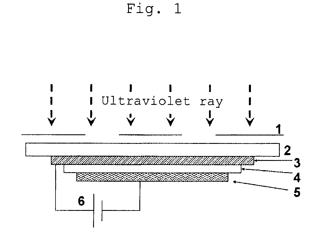
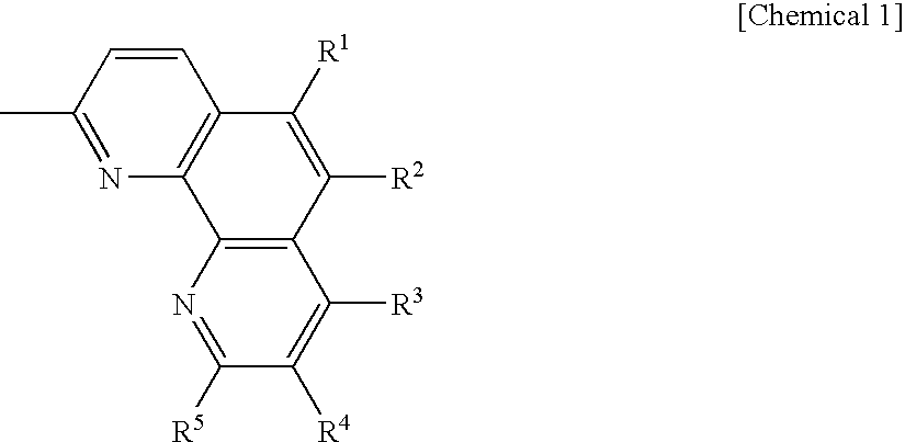
[0080]The organic EL device with a thickness of 10 mm×10 mm having the structure described below was manufactured. Specifically, a transparent electrode having formed thereon an ITO film with a thickness of 150 nm was formed on a glass substrate having a thickness of 0.7 mm. Formed on the transparent electrode were a molybdenum trioxide doped N,N′-di(naphthalene-1-yl)-N,N′-diphenyl benzidine (α-NPD) film with a thickness of 10 nm serving as a hole injecting layer, an α-NPD film with a thickness of 21 nm serving as a hole transporting layer, a film composed of tris(8-quinolynol)aluminum(Alq3) and a compound of 2,3,6,7-tetrahydro-1,1,7,7-tetramethyl-10-(thiazole-2-yl)-1H,5H,11H-[1]benzopyrano[6,7,8-ij]quinolizin-11-one (NKX-1595) expressed by

[0081]

with a thickness of 30 nm serving as a luminous layer, a DPB film having a thickness of 32 nm serving as an electron transporting layer, a film composed of DPB and mono(8-quinolynolate) lithium complex (Liq) with a thickness of 10 nm serving...

examples 2 and 3

[0087]An organic EL device was manufactured in the same manner as in Example 1 except that the thickness of the α-NPD film serving as the hole transporting layer was set to 50 nm (Example 2) or set to 80 nm (Example 3).

[0088]The observation and evaluation of each organic EL device after the irradiation of the ultraviolet ray were performed in the same manner as in Example 1.

[0089]As a result of the visual observation, in case where the ultraviolet ray was irradiated in 1.5 J / cm2 and where the ultraviolet ray was not irradiated, the whole surface of the device emits green light. When the ultraviolet ray was irradiated in 7.5 J / cm2 and 15.0 J / cm2, the green light emission is slightly dark only at the mask opening portion. Compared to Example 1, the green light emission became darker in Example 2, and further darker in Example 3. The green light emission was slightly darker in the case of the irradiation amount of the ultraviolet ray of 15.0 J / cm2 than the case of the irradiation amoun...

example 4

[0104]Ultraviolet ray in an amount of 15.0 J / cm2 was irradiated to the whole surface of the device manufactured in Comparative Example 1 in the same manner as in Example 1, while applying a bias (+7.5 V) between the electrodes of the device, and the brightness reduction was evaluated.

[0105]As a result, the ratio of the brightness after the irradiation of the ultraviolet ray to the brightness when the ultraviolet ray was not irradiated was 83%.


PUM


Abstract

The present invention provides a patterning method of an organic EL device that can easily and efficiently be performed with high definition, and that can control a contrast by a luminous brightness.In an organic EL device having an organic layer, including an organic luminescent material, formed between a pair of counter electrodes, ultraviolet ray is irradiated to the organic layer, and the amount of irradiation is changed to form an emission pattern having a contrast caused by a luminous brightness corresponding to the amount of the irradiation of the ultraviolet ray.

Description

BACKGROUND OF THE INVENTION[0001]1. Field of the Invention[0002]The present invention relates to a patterning method of an organic electroluminescent (hereinafter referred to as organic EL) device in which ultraviolet ray is irradiated to an organic EL device to form a light-emission pattern.[0003]2. Description of the Related Art[0004]An organic EL device is a self-emitting type device employing an organic compound as a luminescent material. It can emit light with high speed, so that it is suitable for a display of a moving image. Further, an organic EL device has a characteristic that its device structure is simple, which makes it possible to reduce a size of a display panel. Since the organic EL device has such an excellent characteristic, it has been spreading in daily life for use in a cellular phone, or a vehicle-mounted display.[0005]There has conventionally been a method of coloring a cathode layer with the use of a mask, or a method of insulation using a resist, as a method...

Claims


Application Information

Patent Timeline
Patent Type & Authority Patents(United States)
IPC IPC(8): H05B33/10H01J9/227
CPCH01L51/0015H01L51/0072H01L51/0081H01L51/5048Y02E10/549Y02P70/50H10K71/211H10K85/324H10K85/6572H10K50/14H10K30/00
Inventor KAWAI, TAKASHIODA, ATSUSHI
Owner YAMAGATA PROMOTIONAL ORG FOR INDAL TECH
Why Eureka
Try Eureka