Single and few-layer graphene based photodetecting devices

a graphene and photodetecting technology, applied in the field of photodetectors, can solve the problems of less than optimal photodetectors, limited intrinsic bandwidth of semiconductor based photodetectors, and inability to detect photons

Active Publication Date: 2011-11-08
GLOBALFOUNDRIES U S INC
View PDF12 Cites 44 Cited by
  • Summary
  • Abstract
  • Description
  • Claims
  • Application Information

AI Technical Summary

Benefits of technology

[0007]According to another aspect, multiple photodetection elements can be provided along with conventional signal processing readout circuitry to create a photodetecting array.

Problems solved by technology

Semiconductor materials, however, have a band gap, and therefore only photons having energy greater than the band gap can be detected, potentially leaving photons undetected.
In addition, the intrinsic bandwidth of semiconductor based photodetectors is limited by the carrier transit time in the photodetection region.
Both of these limitations results in a less than optimal photodetector.

Method used


Image

  • Single and few-layer graphene based photodetecting devices
  • Single and few-layer graphene based photodetecting devices
  • Single and few-layer graphene based photodetecting devices

Examples


Embodiment Construction

[0015]The embodiments herein and the various features and advantageous details thereof are explained more fully with reference to the non-limiting embodiments that are illustrated in the accompanying drawings and detailed in the following description. Descriptions of well-known components and processing techniques are omitted so as to not unnecessarily obscure the embodiments herein. Conventional processes well known in semiconductor processing can be utilized in fabricating the structures described herein. The examples used herein are intended merely to facilitate an understanding of ways in which the embodiments herein may be practiced and to further enable those of skill in the art to practice the embodiments herein. Accordingly, the examples should not be construed as limiting the scope of the embodiments herein.

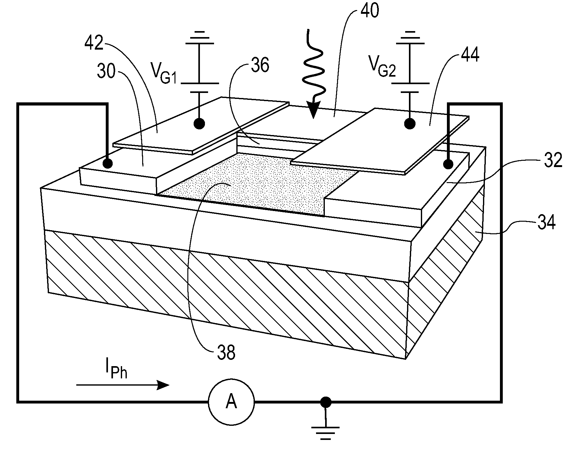
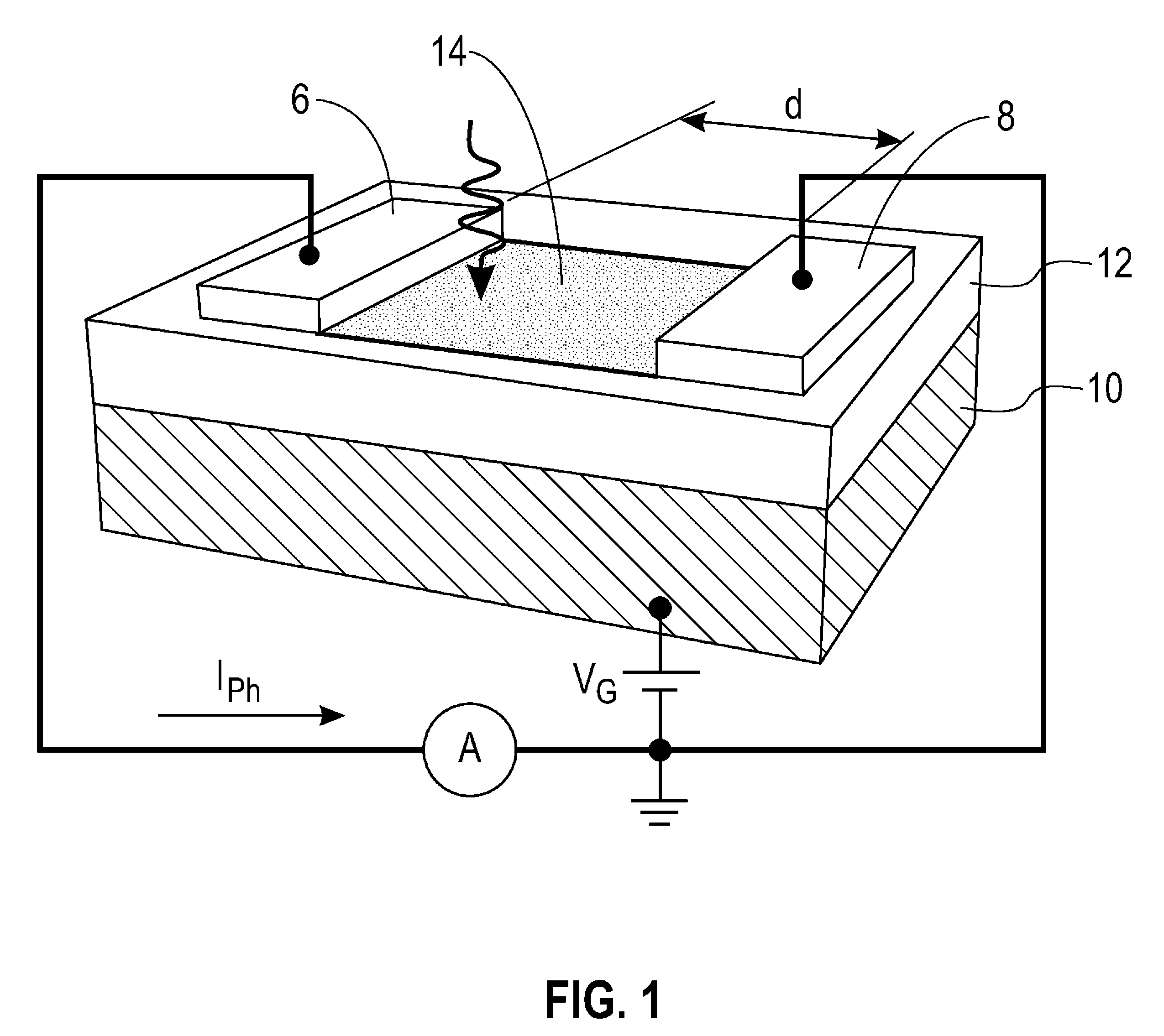
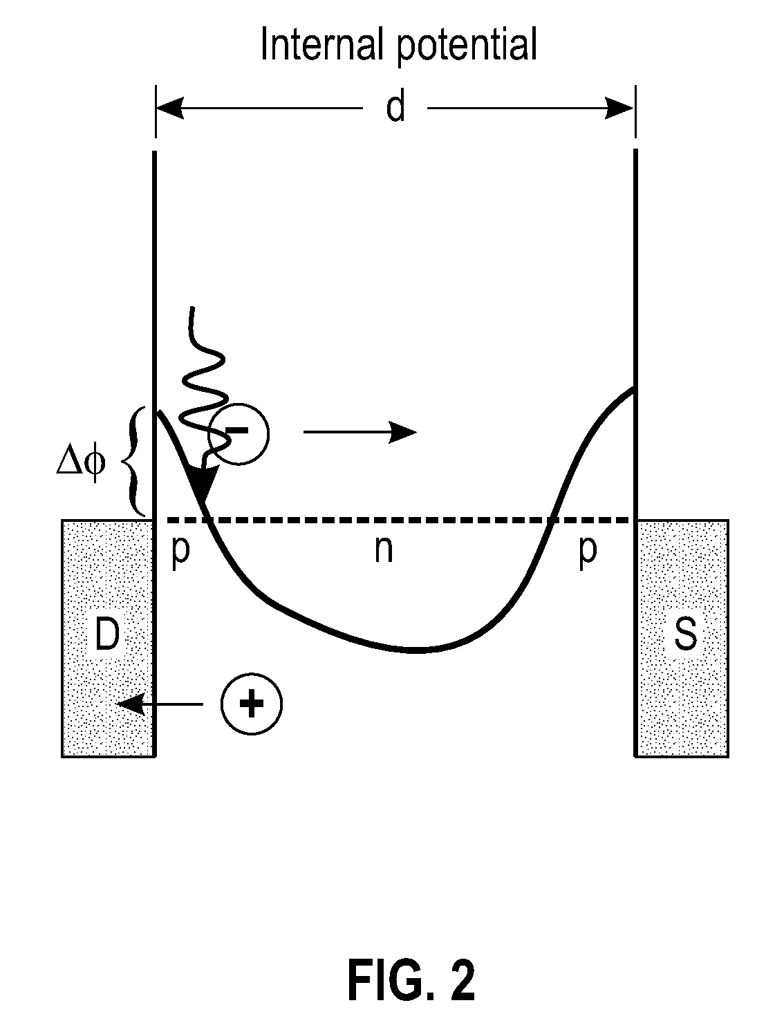
[0016]The present invention is the use of single or multi-layer graphene as the photodetecting layer in a photodetector. Because of graphene's unique property of being a...


PUM


Abstract

A photodetector which uses single or multi-layer graphene as the photon detecting layer is disclosed. Multiple embodiments are disclosed with different configurations of electrodes. In addition, a photodetector array comprising multiple photodetecting elements is disclosed for applications such as imaging and monitoring.

Description

FIELD OF THE INVENTION[0001]The present invention is a photodetector which uses single or multi-layer graphene as the photon detecting layer.BACKGROUND[0002]Photodetectors are used to detect or sense light or other electromagnetic energy. Currently available photodetectors are generally used in a variety of practical applications such as wired and wireless communications, sensing, monitoring, scientific instrumentations, national security, and so on.[0003]Many optical photodetectors use semiconductor materials as the photodetection material system. Semiconductor materials, however, have a band gap, and therefore only photons having energy greater than the band gap can be detected, potentially leaving photons undetected. In addition, the intrinsic bandwidth of semiconductor based photodetectors is limited by the carrier transit time in the photodetection region. Both of these limitations results in a less than optimal photodetector.BRIEF SUMMARY[0004]The present invention provides a ...

Claims


Application Information

Patent Timeline
Patent Type & Authority Patents(United States)
IPC IPC(8): H01L29/15
CPCH01L29/1606H01L51/428Y02E10/549H01L31/02327H01L31/035209H01L31/101Y02P70/50H10K30/65
Inventor AVOURIS, PHAEDONLIN, YU-MINGMUELLER, THOMASXIA, FENGNIAN
Owner GLOBALFOUNDRIES U S INC
Why Eureka
Try Eureka