
Method and apparatus for displaying image signal

a technology of image signal and display method, applied in image analysis, image enhancement, instruments, etc., can solve the problems of inability to provide exact sub-pixel blending, color error bands are most noticeable, and not ideal for every application, so as to reduce the number of color error bands and increase the pixel size

Active Publication Date: 2011-11-22
SAMSUNG ELECTRONICS CO LTD
View PDF38 Cites 5 Cited by
  • Summary
  • Abstract
  • Description
  • Claims
  • Application Information

AI Technical Summary

Benefits of technology

The solution effectively reduces color error bands, improving image definition at edges and boundaries, applicable to displays with striped sub-pixel structures like PDPs, LCDs, and OLEDs.

Problems solved by technology

The RGB model makes design of a computer graphic system simple, but it is not ideal for every application.
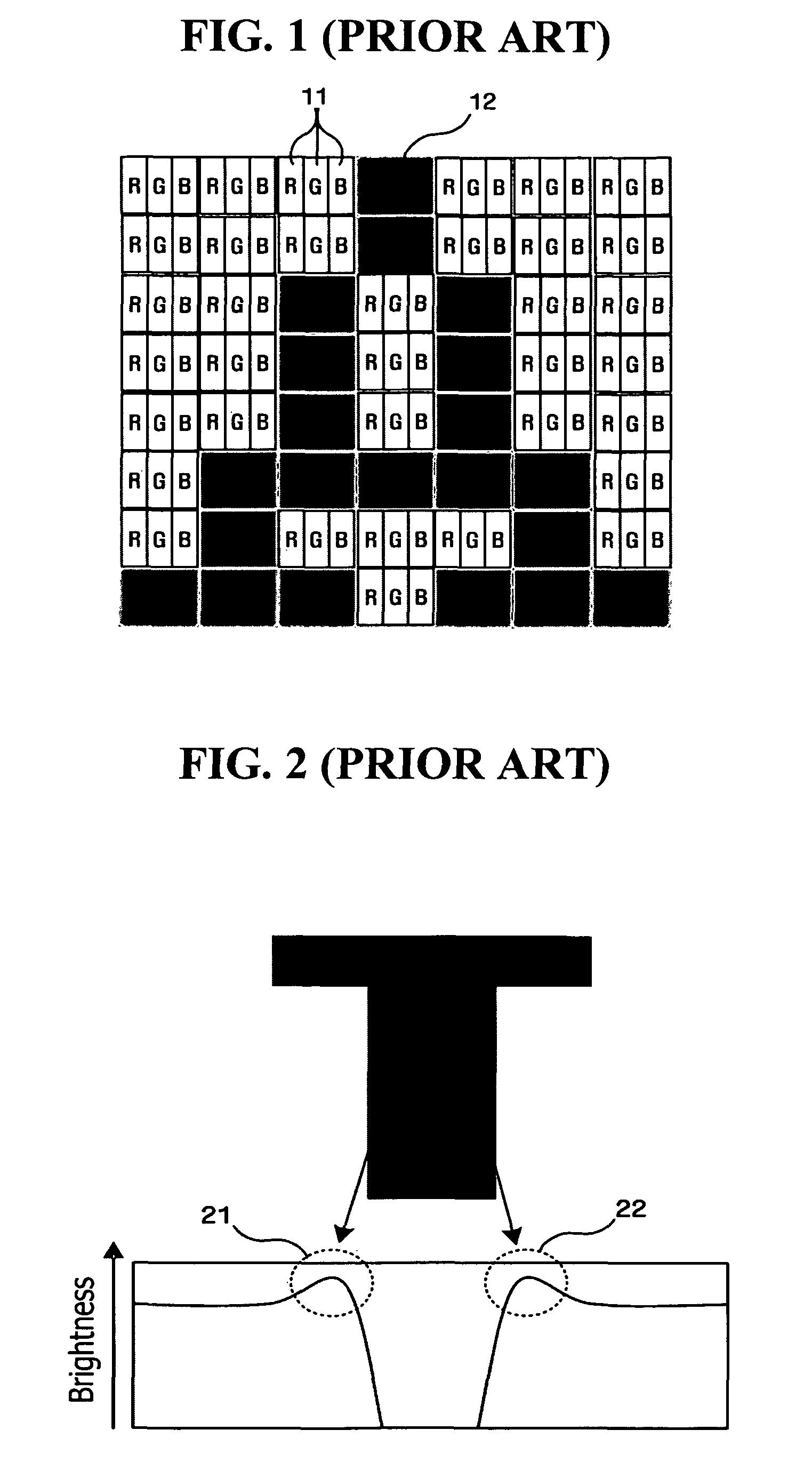
However, since the RGB sub-pixels respectively occupy different spaces, a problem occurs in that exact sub-pixel blending may not be provided.
Particularly, this problem is most noticeable in the case of a large-sized pixel or at the boundary between pixels.
These color error bands are most noticeable when the pixel is large.

Method used


Image

  • Method and apparatus for displaying image signal
  • Method and apparatus for displaying image signal
  • Method and apparatus for displaying image signal

Examples


first embodiment

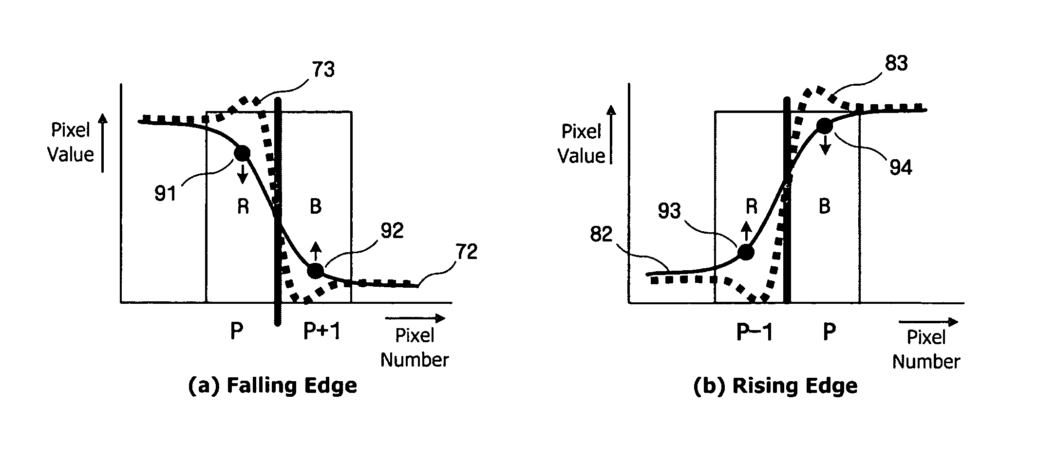
[0045]In the first embodiment, a method of changing a distorted sub-pixel component only is suggested as shown in FIG. 9. At the falling edge shown in (a) of FIG. 9, R component 91 of an input signal 72 is corrected to be decreased by a predetermined value so that an increased output pixel value can be corrected, while B component 92 of the input signal 72 is corrected to be increased by a predetermined value so that a decreased output pixel value can be corrected.

[0046]The decreased R component (R′) can be expressed as Equation (2) while the increased B component (B′) can be expressed as Equation (3). It is noted from Equation (2) that the correction range increases as the difference between current sub-pixels R(p) and B(p) and next sub-pixels R(p+1) and B(p+1) increases.

R′=α×{R(p)−R(p+1)}+R(p+1)  (2)

B′=β×{B(p)−B(p+1)}+B(p+1)  (3)

[0047]In Equation (2) and Equation (3), α and β are factors for determining the correction range and have a constant value between 0 and 1. The sum of α a...

second embodiment

[0049]In the second embodiment, a method of changing sub-pixel components adjacent to a distorted sub-pixel component while maintaining the distorted sub-pixel component is suggested as shown in FIG. 10. At the falling edge shown in (a) of FIG. 10, B and G components 101 which are sub-pixels adjacent to R component 91 are corrected to be increased by a predetermined value, whereby the B and G components become a similar level to the increased R component. An increased correction range of the B and G components 101 can have a value equal to a correction range obtained by Equation (2), i.e., |R′−R(p)|.

[0050]Likewise, G and R components 102 which are sub-pixels adjacent to B component 92 are corrected to be decreased by a predetermined value, whereby the G and R components become a similar level to the decreased B component. An decreased correction range of the G and R components 102 can have a value equal to a correction range obtained by Equation (3), i.e., |B′−B(p)|.

[0051]Meanwhile,...

third embodiment

[0053]In the third embodiment implemented by combination of the first embodiment and the second embodiment, a method of changing both a distorted sub-pixel component and sub-pixel components adjacent to the distorted sub-pixel component is suggested as shown in FIG. 11.

[0054]First, at the falling edge shown in (a) of FIG. 11, R component 91 is corrected to be decreased by a predetermined value and B and G components 101 which are sub-pixels adjacent to the R component 91 are corrected to be increased by a predetermined value, whereby all the components have the same level as one another.

[0055]For example, the decreased correction range is equal to the correction range of Equation (2), i.e., a value obtained by multiplying |R′−R(p)| and a predetermined coefficient γ while the increased correction range is equal to a value obtained by multiplying |R′−R(p)| and 1−γ, wherein γ has a constant value between 0 and 1. The third embodiment becomes identical with the first embodiment if γ is ...


PUM


Abstract

A method and apparatus for reducing color error bands occurring due to the abrupt difference in brightness between sub-pixels. In the method of displaying an image signal of an apparatus for displaying the image signal, the apparatus includes a plurality of pixels each having at least two sub-pixels, and the method includes detecting pixels that belong to an edge of an input image, changing pixel values of the sub-pixels constituting the pixels belonging to the edge, and driving a display in accordance with the new pixel value.

Description

CROSS-REFERENCE TO RELATED APPLICATIONS[0001]This application is based on and claims priority from Korean Patent Application No. 10-2005-0074418, filed on Aug. 12, 2006, the disclosure of which is incorporated herein in its entirety by reference.BACKGROUND OF THE INVENTION[0002]1. Field of the Invention[0003]The present invention relates to a method and apparatus for displaying an image signal, and, more particularly, to a method and apparatus for reducing color error bands occurring due to the abrupt difference in brightness between sub-pixels in an apparatus for displaying an image signal, such as a liquid crystal display (LCD), a plasma display panel (PDP), a light-emitting diode (LED), or an organic light emitting diode (OLED).[0004]2. Description of the Related Art[0005]A color space is a model for representing color numerically in terms of three or more coordinates. Different image processing systems employ different color spaces for different reasons. At present, most apparat...

Claims


Application Information

Patent Timeline
Patent Type & Authority Patents(United States)
IPC IPC(8): G09G5/00
CPCG06T2207/20192G06T2207/10016G09G2340/06G09G5/02G09G3/36G09G2320/103G06T2207/10024G06T2207/20012G09G3/3208G09G2300/0452G09G2340/0457G09G2320/0242G06T5/001G09G5/22G06T5/008G06T5/94H04N9/12G02F1/133
Inventor CHOE, WON-HEEPARK, DU-SIK
Owner SAMSUNG ELECTRONICS CO LTD
Learn More