Method for manufacturing electro-optical device wherein an electrostatic protection circuit is shielded by a light-shielding sheet that is separate and apart from the electro-optical device

a technology of electrostatic protection circuit and light shielding sheet, which is applied in the direction of circuit electrostatic discharge protection, optics, instruments, etc., can solve the problems of increased power consumption of liquid crystal devices, damage to elements of driving circuits that are arranged outside the pixel region of element substrates, and low power consumption

Active Publication Date: 2011-11-22
JAPAN DISPLAY WEST
View PDF19 Cites 9 Cited by
  • Summary
  • Abstract
  • Description
  • Claims
  • Application Information

AI Technical Summary

Benefits of technology

[0012]Since the electrostatic protection circuit is shielded from UV light during the formation of the molding member, current-voltage properties of the diode elements are prevented from being varied. This prevents currents from leaking through the diode elements; hence, the presence of the electrostatic protection circuit does not lead to an increase in powder consumption.
[0030]In the third example, it is particularly effective that electro-optical device includes memory elements each corresponding to one of the pixels. Leakage currents caused by irradiating the diode elements with UV light do not cause an increase in the powder consumption of liquid crystal devices including a plurality of pixels including no memory elements but cause an increase in the powder consumption of the electro-optical device, which include the pixels including the memory elements, because the electro-optical device has low powder consumption. According to the present invention, the following object can be achieved: an object that the power consumption of the electro-optical device is reduced by providing the memory circuits in the pixels.

Problems solved by technology

This leads to low power consumption.
In the liquid crystal device, elements of the driving circuit that are arranged outside a pixel region of the element substrate may be damaged by static electricity while the liquid crystal device is in-process or after the liquid crystal device is completed.
Hence, the following problem cannot occur: a problem in that the liquid crystal device has increased power consumption.
However, the inventors have found that the liquid crystal device including the electrostatic protection circuit has a power consumption greater than that of a liquid crystal device including no electrostatic protection circuit.
This leads to an increase in power consumption.
Such current leakage hardly causes an increase in the power consumption of conventional liquid crystal devices each including a plurality of pixels having no memory elements.
However, the leakage of the micro-currents from the diode elements leads to an increase in the power consumption of the liquid crystal device including the electrostatic protection circuit because the pixels of this liquid crystal device each include a memory element and therefore this liquid crystal device has low power consumption.
Leakage currents caused by irradiating the diode elements with UV light do not cause an increase in the powder consumption of liquid crystal devices including a plurality of pixels including no memory elements but cause an increase in the powder consumption of the electro-optical device, which include the pixels including the memory elements, because the electro-optical device has low powder consumption.
This is because the UV light, applied to the second surface of the element substrate, for curing the UV-curable molding member cannot pass through the element substrate and therefore cannot reach the diode elements.
However, the leakage of micro-currents from the diode elements leads to an increase in the powder consumption of the electro-optical device because the electro-optical device, which includes the memory elements correspond to the pixels, has low powder consumption.
Leakage currents caused by irradiating the diode elements with UV light do not cause an increase in the powder consumption of liquid crystal devices including a plurality of pixels including no memory elements but cause an increase in the powder consumption of the electro-optical device, which include the pixels including the memory elements, because the electro-optical device has low powder consumption.

Method used


Image

  • Method for manufacturing electro-optical device wherein an electrostatic protection circuit is shielded by a light-shielding sheet that is separate and apart from the electro-optical device
  • Method for manufacturing electro-optical device wherein an electrostatic protection circuit is shielded by a light-shielding sheet that is separate and apart from the electro-optical device
  • Method for manufacturing electro-optical device wherein an electrostatic protection circuit is shielded by a light-shielding sheet that is separate and apart from the electro-optical device

Examples


first embodiment

Configuration of Electro-Optical Device

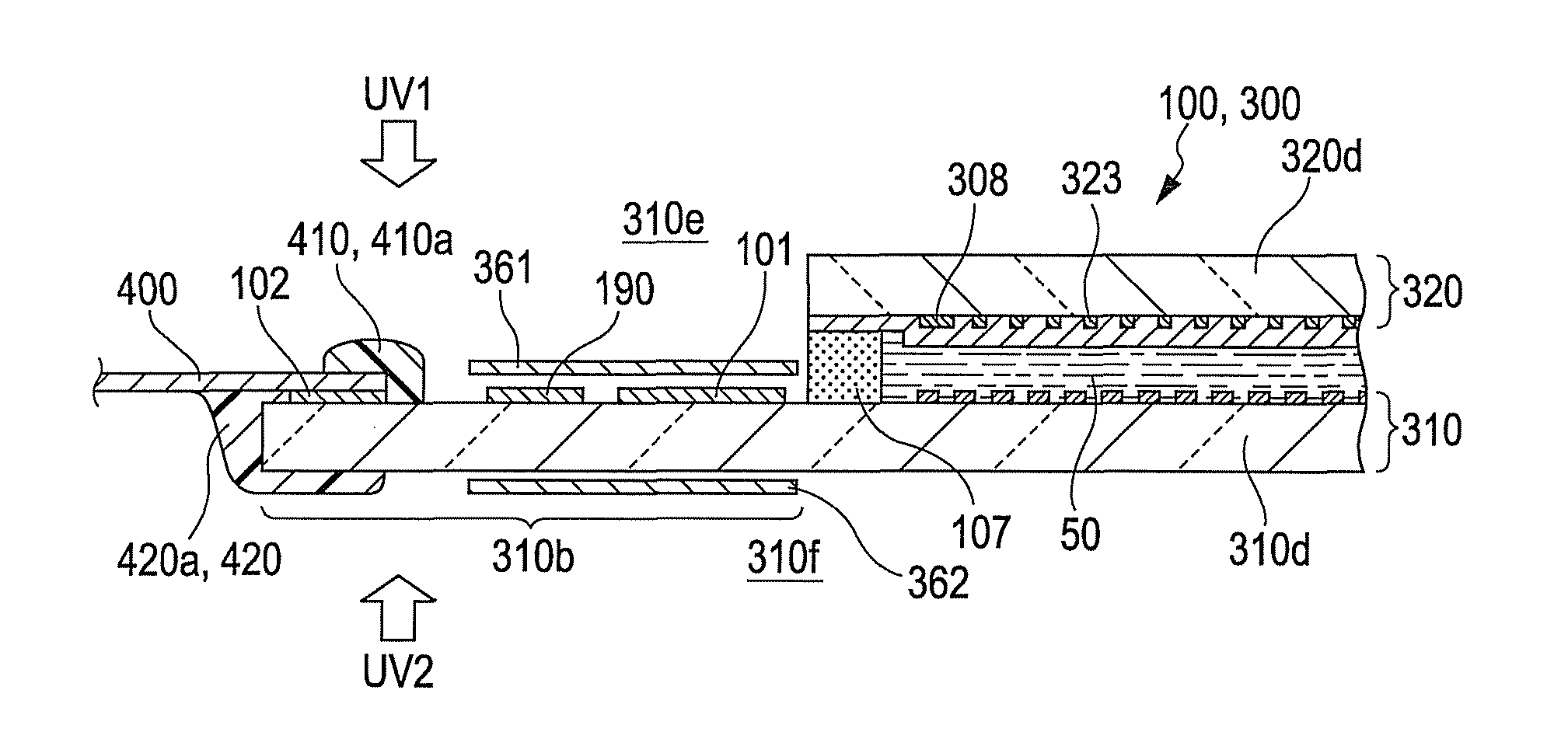
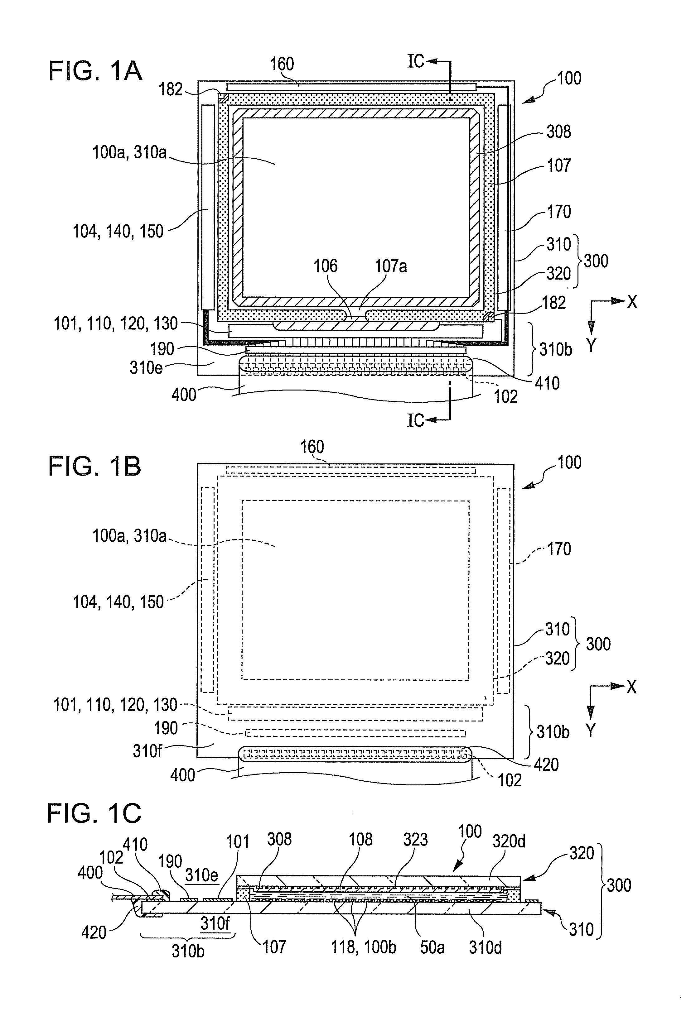
[0050]FIG. 1A is a plan view of an electro-optical device 100 according to a first embodiment of the present invention. FIG. 1B is a bottom view of the electro-optical device 100. FIG. 1C is a sectional view of the electro-optical device 100 taken along the line IC-IC of FIG. 1A. The spatial relationships of members shown in FIG. 1B agree with those of the members shown in FIG. 1A.

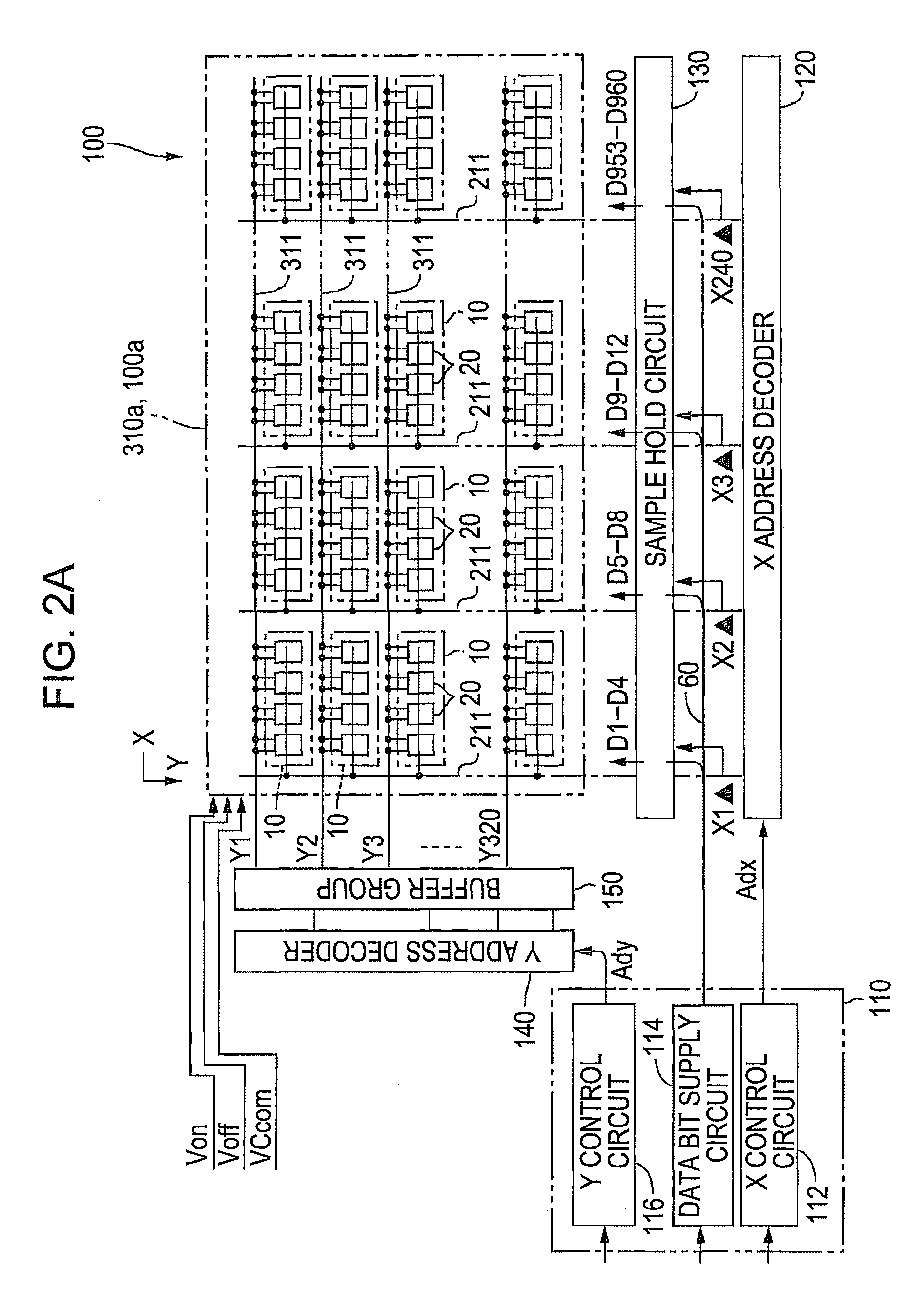
[0051]With reference to FIGS. 1A to 1C, the electro-optical device 100 includes a liquid crystal panel 300. The liquid crystal panel 300 includes a sealing member 107 made of a heat- or UV-curable resin, an element substrate 310 (a first substrate), a counter substrate 320 (a second substrate) bonded to the element substrate 310 with the sealing member 107 with a predetermined space located therebetween, and a liquid crystal layer 50a which is held in a region surrounded by the sealing member 107 and which contains a twisted nematic (TN) liquid crystal 105. The sealin...

second embodiment

[0110]FIG. 7A is a plan view of an electro-optical device 100 according to a second embodiment of the present invention. FIG. 7B is a bottom view of the electro-optical device 100. FIG. 7C is a sectional view of the electro-optical device 100 taken along the line VIIC-VIIC of FIG. 7A. The spatial relationships of members shown in FIG. 7B agree with those of the members shown in FIG. 7A. The configuration of the electro-optical device 100 is the same as that described in the first embodiment with reference to FIGS. 1A to 1C and therefore will not be described in detail.

[0111]The electrical configuration and operation of the electro-optical device 100 is the same as those described in the first embodiment with reference to FIGS. 2 and 3 and therefore will not be described in detail. The configuration of an element substrate 310 is the same as that described in the first embodiment with reference to FIG. 4 and therefore will not be described in detail. The configuration of an electrost...

third embodiment

[0120]FIG. 10A is a plan view of an electro-optical device 100 according to a third embodiment of the present invention. FIG. 10B is a bottom view of the electro-optical device 100. FIG. 10C is a sectional view of the electro-optical device 100 taken along the line XC-XC of FIG. 10A. The spatial relationships of members shown in FIG. 10B agree with those of the members shown in FIG. 10A. The configuration of the electro-optical device 100 is the same as that described in the first embodiment with reference to FIGS. 1A to 1C and therefore will not be described in detail.

[0121]The electrical configuration and operation of the electro-optical device 100 is the same as those described in the first embodiment with reference to FIGS. 2 and 3 and therefore will not be described in detail. The configuration of an element substrate 310 is the same as that described in the first embodiment with reference to FIG. 4 and therefore will not be described in detail. The configuration of an electros...


PUM

PropertyMeasurementUnit
distanceaaaaaaaaaa
areaaaaaaaaaaa
currentaaaaaaaaaa

Abstract

A method for manufacturing an electro-optical device including an element substrate which includes a plurality of pixels including pixel electrodes and which is connected to a circuit board includes providing a UV-curable molding member on the element substrate such that the molding member extends from the element substrate to the circuit board and also includes curing the molding member by irradiating the molding member with UV light. The element substrate includes an electrostatic protection circuit. The electrostatic protection circuit is shielded from the UV light applied to the molding member in the operation of curing the molding member.

Description

CROSS-REFERENCE TO RELATED APPLICATIONS[0001]This application claims the benefit and priority of Japanese Patent Application Nos. 2007-068076, filed Mar. 16, 2007; 2007-068077, filed Mar. 16, 2007; 2007-068078, filed Mar. 16, 2007; 2007-068082, filed Mar. 16, 2007; and 2007-197022, filed Jul. 30, 2007. The entire disclosure of each of the above applications are incorporated herein by reference.BACKGROUND[0002]1. Technical Field[0003]The present invention relates to an electro-optical device including an element substrate with terminals connected to an external circuit board such as a flexible printed circuit board, a method for manufacturing the electro-optical device, and an electronic apparatus including the electro-optical device.[0004]2. Related Art[0005]Among various electro-optical devices, a liquid crystal device includes an element substrate having a plurality of pixels including pixel electrodes; a sealing member; a counter substrate bonded to the element substrate with the...

Claims


Application Information

Patent Timeline
Patent Type & Authority Patents(United States)
IPC IPC(8): G02F1/1345G02F1/1333
CPCG02F1/13452H05K1/0259G02F1/136204G02F2202/023H01L27/0248H05K1/181H05K3/284H05K3/361H05K2201/10977H05K2203/304
Inventor KATAYAMA, SHIGENORIONOGI, TOMOHIDEIMAO, KAZUHIRO
Owner JAPAN DISPLAY WEST
Why Eureka
Try Eureka