Semiconductor structure and method of forming the same

a technology of silicon oxide and semiconductors, applied in the direction of resistors, diodes, semiconductor devices, etc., can solve the problems of leakage current and thin gate insulation layer of silicon oxide, and achieve the effect of simple forming methods

Active Publication Date: 2012-01-10
UNITED MICROELECTRONICS CORP
View PDF9 Cites 13 Cited by
  • Summary
  • Abstract
  • Description
  • Claims
  • Application Information

AI Technical Summary

Benefits of technology

[0006]The present invention provides a semiconductor structure and a method of forming the same. The formed resistor does not include any metal layer to deviate the performance thereof, and the forming method is simple without adding any extra mask.
[0023]In view of above, the resistor of the present invention does not include any metal layer, and the current flows through the polysilicon layer instead of the metal layer, so that the resistance thereof is not degraded. Further, the method of removing the metal layer in the resistor area can be completed with the existing mask and no extra mask is needed. Therefore, the fabrication cost is saved and the competitive advantage is achieved.

Problems solved by technology

However, a leakage current occurs when the gate insulation layer of silicon oxide becomes thinner.

Method used


Image

  • Semiconductor structure and method of forming the same
  • Semiconductor structure and method of forming the same
  • Semiconductor structure and method of forming the same

Examples


Embodiment Construction

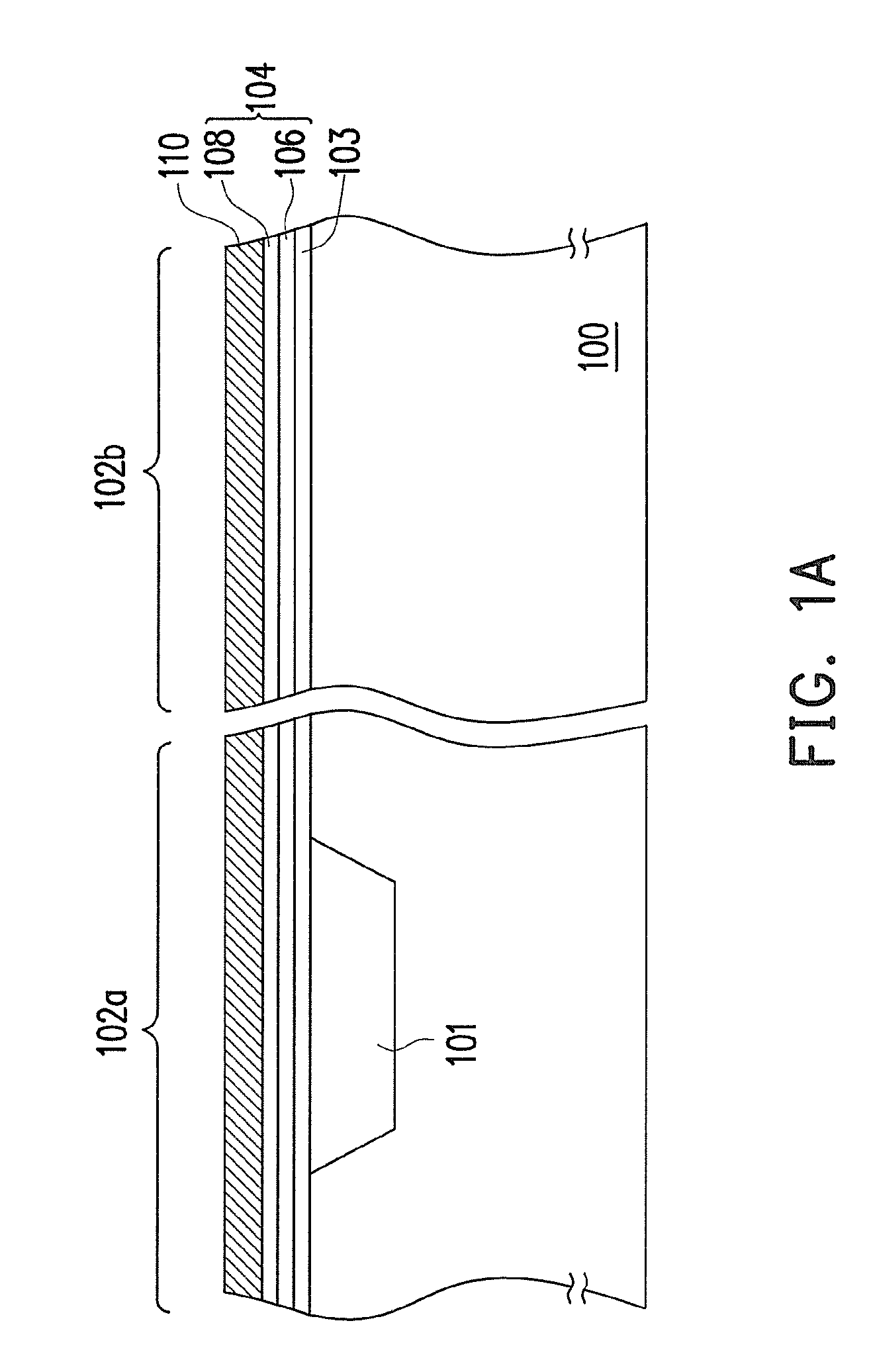
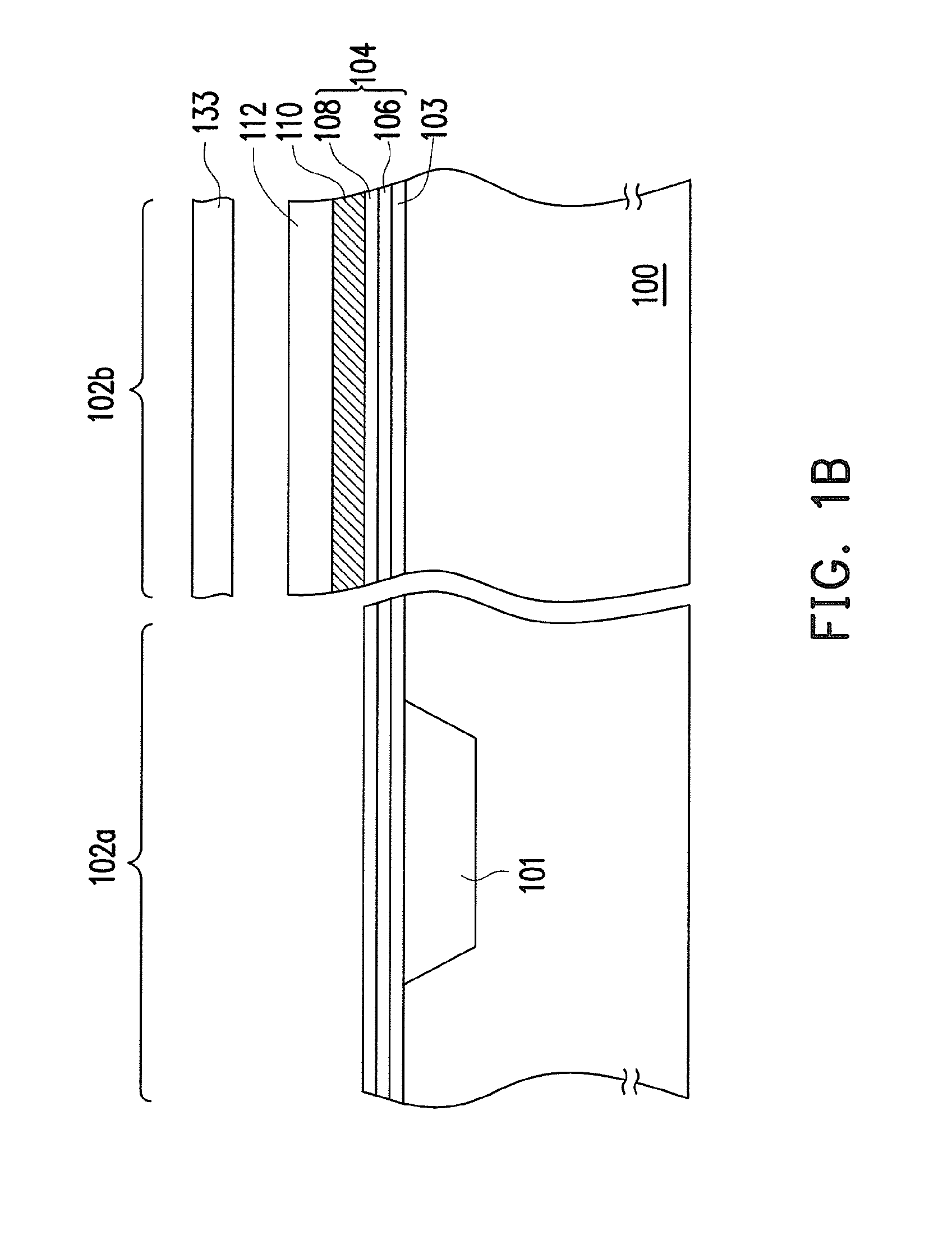
[0027]FIGS. 1A to 1F schematically illustrate, in a cross-sectional view, a method of forming a semiconductor structure according to an embodiment of the present invention.

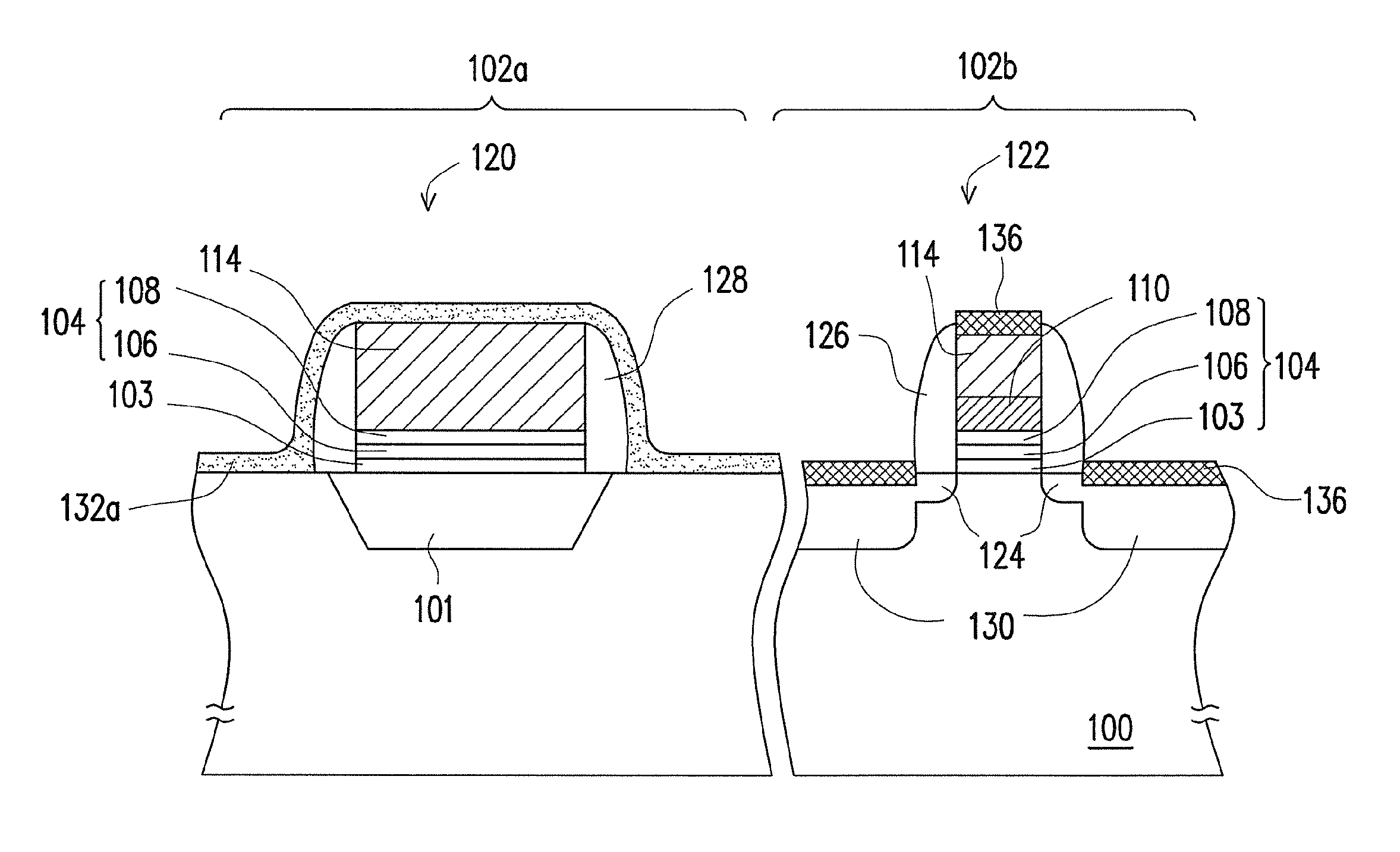
[0028]Referring to FIG. 1A, a substrate 100 is provided. The substrate is a semiconductor substrate such as a silicon substrate, for example. The substrate 100 has a first area 102a for forming a resistor and a second area 102b for forming a MOS transistor. Further, a shallow trench isolation (STI) structure 101 is formed in the substrate 100 in the first area 102a. Thereafter, a dielectric layer 104 and a metal layer 110 are sequentially formed over the substrate 100 in the first area 102a and the second area 102b. The dielectric layer 104 is a stacked structure including a high-k layer 106 and a cap layer 108 sequentially formed on the substrate 100. The high-k layer 106 includes a dielectric material with a dielectric constant greater than 4, for example. The high-k layer 106 includes HfO2, ZrO2, Al2O3, AlN, Ti...


PUM


Abstract

A semiconductor structure and a method of forming the same are provided. The semiconductor structure includes a substrate, a resistor and a metal gate structure. The substrate has a first area and a second area. The resistor is disposed in the first area, wherein the resistor does not include any metal layer. The metal gate structure is disposed in the second area.

Description

BACKGROUND OF THE INVENTION[0001]1. Field of Invention[0002]The present invention relates to a semiconductor structure and a method of forming the same, and more generally to a semiconductor structure including a resistor and a metal gate structure and a method of forming the same.[0003]2. Description of Related Art[0004]As the dimension of a semiconductor device is getting smaller, the dimension of the gate structure and the thickness of the gate insulation layer are reduced accordingly. However, a leakage current occurs when the gate insulation layer of silicon oxide becomes thinner. To reduce the leakage current, a high dielectric constant (high-k) material is used to replace silicon oxide for forming the gate insulation layer. The gate of polysilicon may react with the high-k material to generate a Fermi-level pinning, so that the threshold voltage is increased and the performance of the device is affected. Therefore, a metal layer (i.e. so-called work function metal layer) is u...

Claims


Application Information

Patent Timeline
Patent Type & Authority Patents(United States)
IPC IPC(8): H01L21/337H01L21/8234H01L21/20
CPCH01L21/28088H01L27/0629H01L28/20H01L29/4966H01L29/513H01L29/517H01L29/665H01L29/6659H01L29/7833
Inventor TSENG, KUN-SZUHSU, CHE-HUAFAN, CHENG-WENTSENG, CHIH-YULIANG, VICTOR CHIANG
Owner UNITED MICROELECTRONICS CORP
Why Eureka
Try Eureka