System and method for compartmental shielding of stacked packages

a technology of stacked packages and shielding, applied in the field of radio frequency shielding, can solve the problem of increasing the footprint of semiconductor packages

Active Publication Date: 2012-01-24
AMKOR TECH SINGAPORE HLDG PTE LTD
View PDF36 Cites 41 Cited by
  • Summary
  • Abstract
  • Description
  • Claims
  • Application Information

AI Technical Summary

Problems solved by technology

Side by side solutions requires additional space and th

Method used


Image

  • System and method for compartmental shielding of stacked packages
  • System and method for compartmental shielding of stacked packages
  • System and method for compartmental shielding of stacked packages

Examples


Embodiment Construction

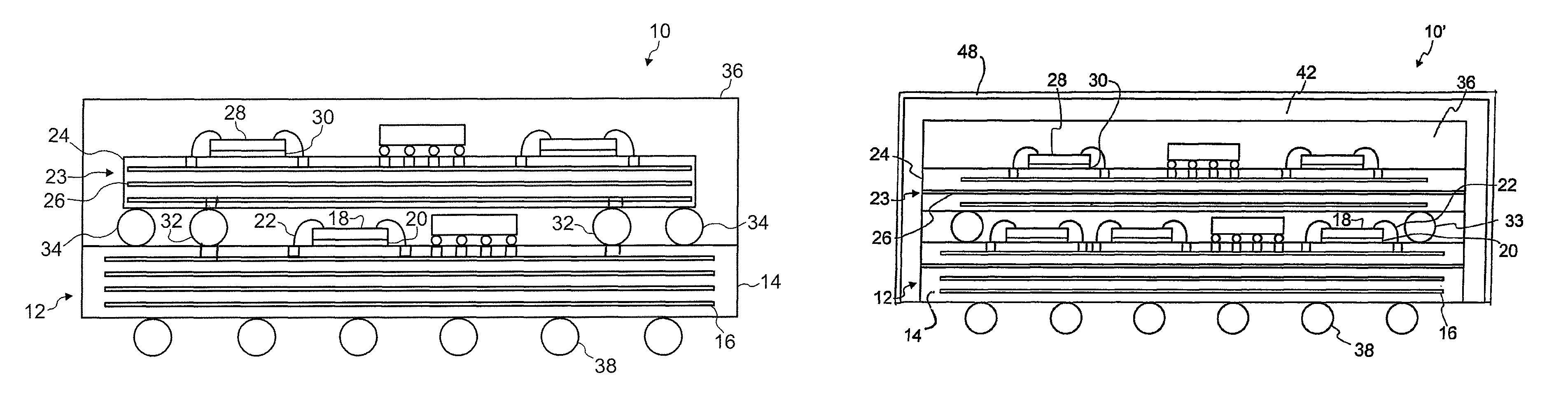
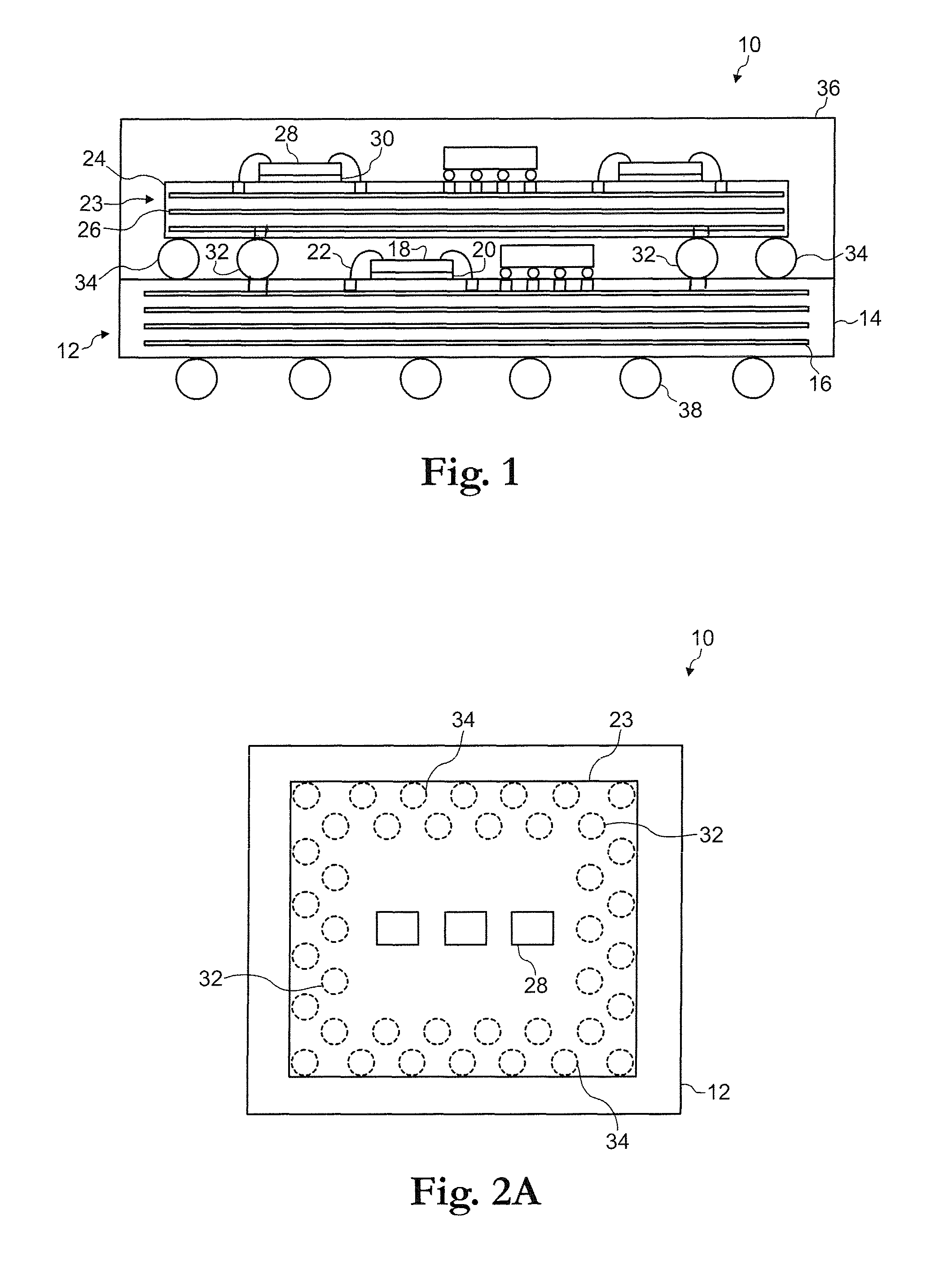
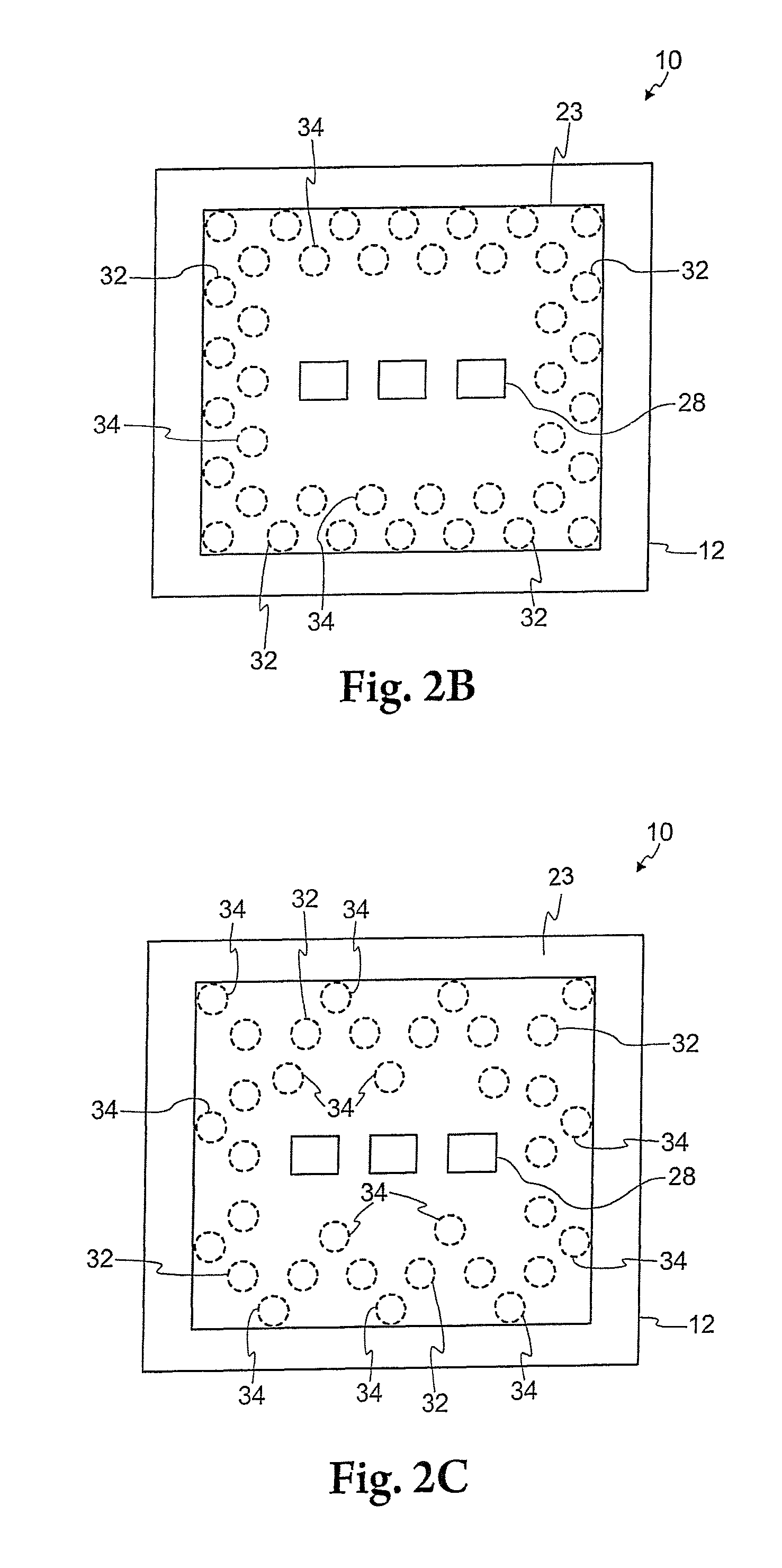
[0017]Referring to FIGS. 1 and 2A, a semiconductor device 10 (hereinafter device 10) is shown. The device 10 provides compartmental shielding which lessens the footprint of prior art semiconductor devices which use a side by side solution.

[0018]The device 10 has a first substrate 12. The first substrate 12 may be any one chosen from a conventional rigid PCB, a flexible PCB, and an equivalent thereof, but the kind of first substrate 12 is not limited herein. The first substrate 12 includes an insulation layer 14 having predetermined area and thickness. The insulation layer 14 has an approximately planar first surface and an approximately planar second surface opposing the first surface. The first substrate 12 has a plurality of metal traces 16 formed on the first surface of the insulation layer 14. A plurality of metal traces 16 may also be formed on the second surface of the insulation layer 14. The number of metal traces 16 is not limited to the number shown in the Figures. If mult...


PUM


Abstract

A semiconductor device has a first substrate having a plurality of metal traces. At least one electronic component is electrically attached to a first surface of the first substrate. A second substrate has a plurality of metal traces and attached to the first substrate. At least one electronic component is electrically attached to a first surface of the second substrate. An RF shield is formed on the first substrate to minimizing Electro-Magnetic Interference (EMI) radiation and Radio Frequency (RF) radiation to the at least one electronic component on the first substrate to form an RF shield. A mold compound is used for encapsulating the semiconductor device.

Description

FIELD OF THE INVENTION[0001]This invention relates to Radio Frequency (RF) shielding and, more specifically, to a system and method for providing compartmental shielding in a semiconductor package that lessens the footprint of semiconductor packages which use a side by side solution.BACKGROUND OF THE INVENTION[0002]Radio Frequency (RF) shielding may be required on certain semiconductor devices and modules (hereinafter semiconductor device) in order to minimize Electro-Magnetic Interference (EMI) radiation from the semiconductor device. RF shielding is further required to prevent RF radiation from external sources from interfering with operation of the semiconductor device. In a semiconductor device which integrates multiple functions / modules (front end module+transmitter, radio+baseband, etc.) compartmental shielding may be required to minimize EMI radiation from the different components / modules and to prevent RF radiation from interfering with operation of the different components / ...

Claims


Application Information

Patent Timeline
IPC IPC(8): H01L21/56
CPCH01L23/3128H01L23/552H01L25/162H01L2924/3025H01L24/48H01L2924/15331H01L2924/15311H05K2201/042H05K1/144H01L2224/73265H01L2224/48227H01L2224/48091H01L2224/32225H01L2224/16225H01L2924/00014H01L2924/00012H01L2924/00H01L24/73H01L2924/181H01L2224/45099H01L2224/45015H01L2924/207
Inventor BOLOGNIA, DAVIDKELLY, MIKESMITH, LEE
Owner AMKOR TECH SINGAPORE HLDG PTE LTD
Why Eureka
Try Eureka