Semiconductor package and method of manufacturing the same, and semiconductor device and method of manufacturing the same

a semiconductor and package technology, applied in the manufacture of printed circuits, printed circuit aspects, basic electric elements, etc., can solve the problems of lowering the fusing of the solder used to fix the lead pin, and the cradling of the solder head, so as to achieve the effect of enhancing the reliability of the electrical connection of the lead pin, facilitating manufacturing, and sufficient fitting strength of the lead pin

Active Publication Date: 2012-02-21
SHINKO ELECTRIC IND CO LTD
View PDF4 Cites 70 Cited by
  • Summary
  • Abstract
  • Description
  • Claims
  • Application Information

AI Technical Summary

Benefits of technology

[0011]It is an object of the present invention to provide a semiconductor package equipped with lead pins, which can have a sufficient fitting strength and have high reliability of the electrical connection, and a method of manufacturing the same and a semiconductor device and a method of manufacturing the same.
[0014]Accordingly, the lead pin is supported by the projection-shaped resin portion. Therefore, a fitting strength of the lead pin can be improved in contrast to the prior art.
[0017]In the present invention, even in such a case, since the lead pin is supported by the projection-shaped resin portion, it can be prevented that the lead pin is inclined by the reflow of the solder. Also, even though the solder crawls up toward the top end side of the lead pin, the solder is covered with the projection-shaped resin portion. Therefore, there is no chance that the solder whose surface is oxidized is exposed on the surface of the lead pin, and reliability of the electrical connection of the lead pin can be enhanced.
[0019]By employing the manufacturing method of the present invention, the semiconductor package having the above structure can be manufactured easily. As the method of forming the uncured resin layer, a resin film in which the opening corresponding to the lead pin is provided may be pasted, or a liquid resin may be coated by the syringe or the dispenser.
[0020]As explained above, in the present invention, a sufficient fitting strength of the lead pins of the semiconductor package can be obtained, and reliability of the electrical connection of the lead pins can be enhanced.

Problems solved by technology

At a time of the reflow heating of the solder used to mount the semiconductor chip, in some cases, such a situation is caused that the solder used to fix the lead pins is fused and crawls up toward the top end side of the lead pins.
Since a surface of the solder is oxidized, such a problem arises that, when the solder that crawls up toward the top end side of the lead pins constitutes the connecting portion, reliability of the electrical connection of the lead pins is lowered.

Method used


Image

  • Semiconductor package and method of manufacturing the same, and semiconductor device and method of manufacturing the same
  • Semiconductor package and method of manufacturing the same, and semiconductor device and method of manufacturing the same
  • Semiconductor package and method of manufacturing the same, and semiconductor device and method of manufacturing the same

Examples


first embodiment

[0054]FIG. 2 to FIG. 6 are sectional views showing a method of manufacturing a semiconductor package according to a first embodiment of the present invention.

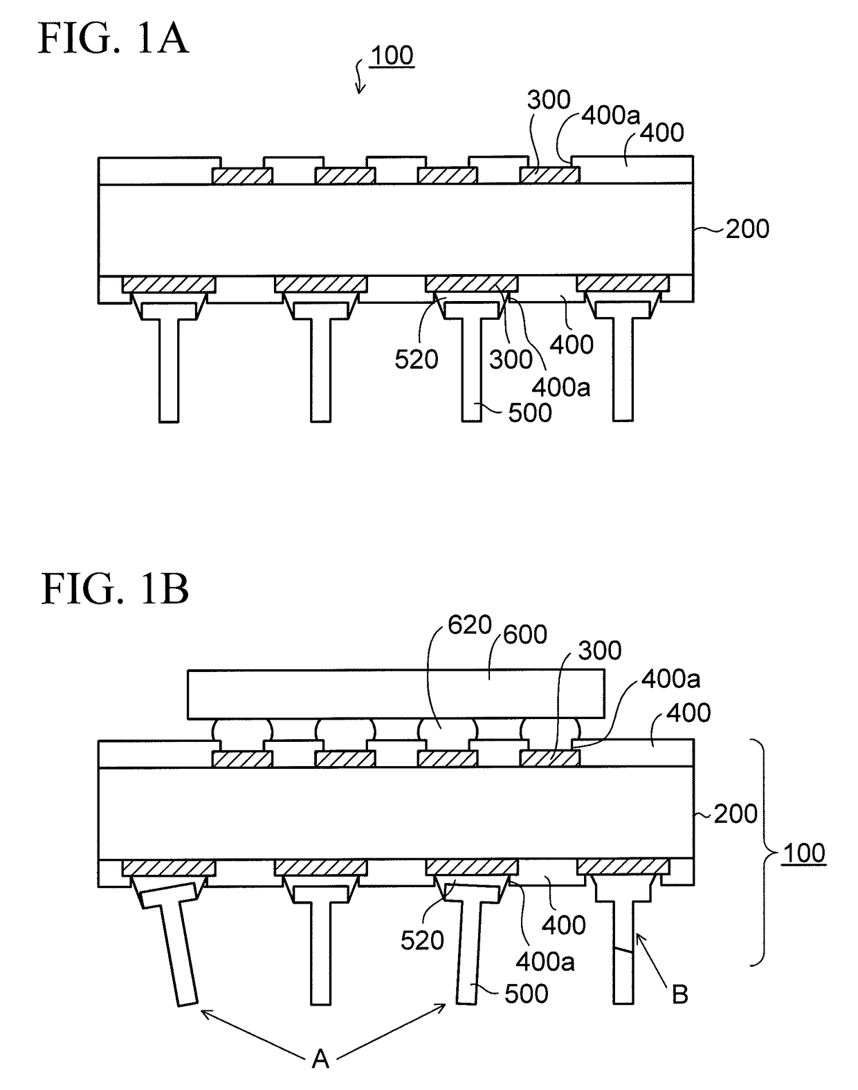
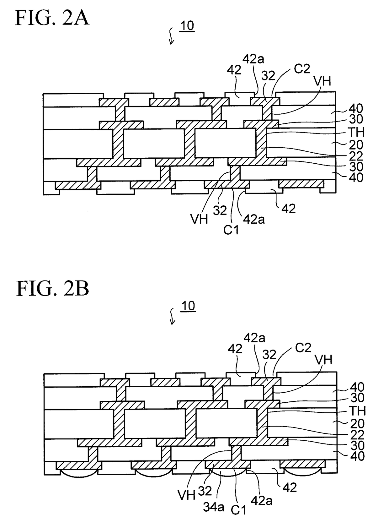
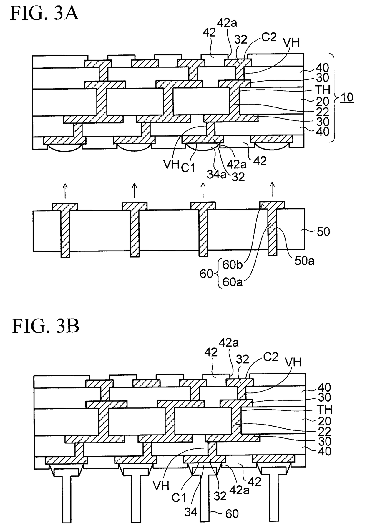
[0055]In the method of manufacturing the semiconductor package of the first embodiment, first, a wiring substrate 10 shown in FIG. 2A is prepared. In the wiring substrate 10, an insulating core substrate 20 made of a glass epoxy resin, or the like is arranged in a center portion in the thickness direction, and through holes TH are provided in the core substrate 20. First wiring layers 30 connected mutually via through electrodes 22 filled in the through holes TH are formed on both surface sides of the core substrate 20 respectively. Otherwise, the first wiring layers 30 on both surface sides may be connected mutually via through hole plating layers (through electrodes) provided on inner walls of the through holes TH in the core substrate 20, and then the remained holes of the through holes TH may be filled with a resin.

[0056]An...

second embodiment

[0093]FIG. 12 to FIG. 15 are sectional views showing a method of manufacturing a semiconductor package according to a second embodiment of the present invention. In the foregoing first embodiment, the reinforcing resin layer 70 is formed of the resin film 70x of a single layer such as an epoxy resin, or the like. Sometimes there is a case that flame retardancy is provided to the surface of the semiconductor package on the lead pin side, but it is difficult to obtain the flame retardancy by the single epoxy resin.

[0094]Also, a rigidity of resin film 70x of the single layer is low. Therefore, such a situation is supposed that its handling during the manufacturing step is not stable and thus the handling becomes difficult. Also, the projection-shaped resin portion 72 is formed by fluidizing resin film 70x of the single layer. Therefore, there is a possibility that a clearance is produced between the lead pin 60 and the projection-shaped resin portion 72, and it is feared that the crawl...

third embodiment

[0128]FIG. 19 and FIG. 20 are fragmental sectional views showing a surrounding structure of a lead pin in a semiconductor package according to a third embodiment of the present invention. A difference of the third embodiment from the second embodiment resides in a shape of the reinforcing resin layer around the lead pins, and remaining elements are similar to those of the second embodiment and shown in FIG. 15. Therefore, explanation will be made with reference to a fragmental sectional view around the lead pin.

[0129]As shown in FIG. 19, in a first example of the third embodiment of the present invention, a filling resin portion 72a of the reinforcing resin layer 70 is filled into the interval d5 between the outer periphery of the lead pin 60 and the side surface of the opening portion 74a in the flame retardant film 74x, and a top surface TS1 (outer surface) of the filling resin portion 72a and the outer surface of the flame retardant film 74x constitute the identical surface (flat...


PUM


Abstract

A semiconductor package of the present invention, includes a wiring substrate, a lead pin fixed to a connection pad on one surface side of the wiring substrate by solder, and a reinforcing resin layer formed on a surface of the wiring substrate on which the lead pin is provided and having a projection-shaped resin portion which projects locally around the lead pin and covers a side surface of a base portion side of the lead pin. The projection-shaped resin portion has a top surface extending from an outer peripheral portion of the lead pin to an outside, and a side surface constituting a non-identical surface to the top surface.

Description

CROSS-REFERENCE TO RELATED APPLICATIONS[0001]This application is based on and claims priority of Japanese Patent Application No. 2008-216325 filed on Aug. 26, 2008, and Japanese Patent Application No. 2008-242066 filed on Sep. 22, 2008, the entire contents of which are incorporated herein by reference.BACKGROUND OF THE INVENTION[0002]1. Field of the Invention[0003]The present invention relates to a semiconductor package and a method of manufacturing the same and a semiconductor device and a method of manufacturing the same and, more particularly, a semiconductor package in which lead pins are fitted to a wiring substrate as connection terminals and a method of manufacturing the same and a semiconductor device and a method of manufacturing the same.[0004]2. Description of the Related Art[0005]In the prior art, there is a semiconductor package having such a structure that lead pins are fitted to a wiring substrate as connection terminals. In such semiconductor package, a semiconductor...

Claims


Application Information

Patent Timeline
Patent Type & Authority Patents(United States)
IPC IPC(8): H01L23/538
CPCH01L21/4853H01L23/49811H05K3/284H01L23/49822H01L23/49827H01L23/49894H01L2224/16225H01L2924/0102H01L2924/01078H01L2924/01079H01L2924/15174H01L2924/15311H01L2924/15312H05K3/4682H05K2201/091H05K2201/10318H05K2201/10977H01L2924/1461H01L2924/00014H01L2924/00011H01L2224/0401
Inventor KOIZUMI, NAOYUKITATEIWA, AKIHIKO
Owner SHINKO ELECTRIC IND CO LTD
Why Eureka
Try Eureka