Multi-power source semiconductor device

a technology of power source semiconductors and power supply circuits, applied in the direction of generating/distributing signals, pulse techniques, instruments, etc., can solve the problem that the delay circuit may increase the delay amoun

Active Publication Date: 2012-02-28
NEC CORP
View PDF28 Cites 12 Cited by
  • Summary
  • Abstract
  • Description
  • Claims
  • Application Information

AI Technical Summary

Benefits of technology

[0023]An object of the present invention is to provide a multi-supply-voltage semiconductor device capable of reducing clock skew between blocks without using a complex configuration, even if a power supply voltage changes in a case where the delay in each clock circuit provided for each block has a different power-supply-voltage dependency.

Problems solved by technology

The variable delay circuit may increase the amount of delay as the power supply voltage decreases.

Method used


Image

  • Multi-power source semiconductor device
  • Multi-power source semiconductor device
  • Multi-power source semiconductor device

Examples


first embodiment

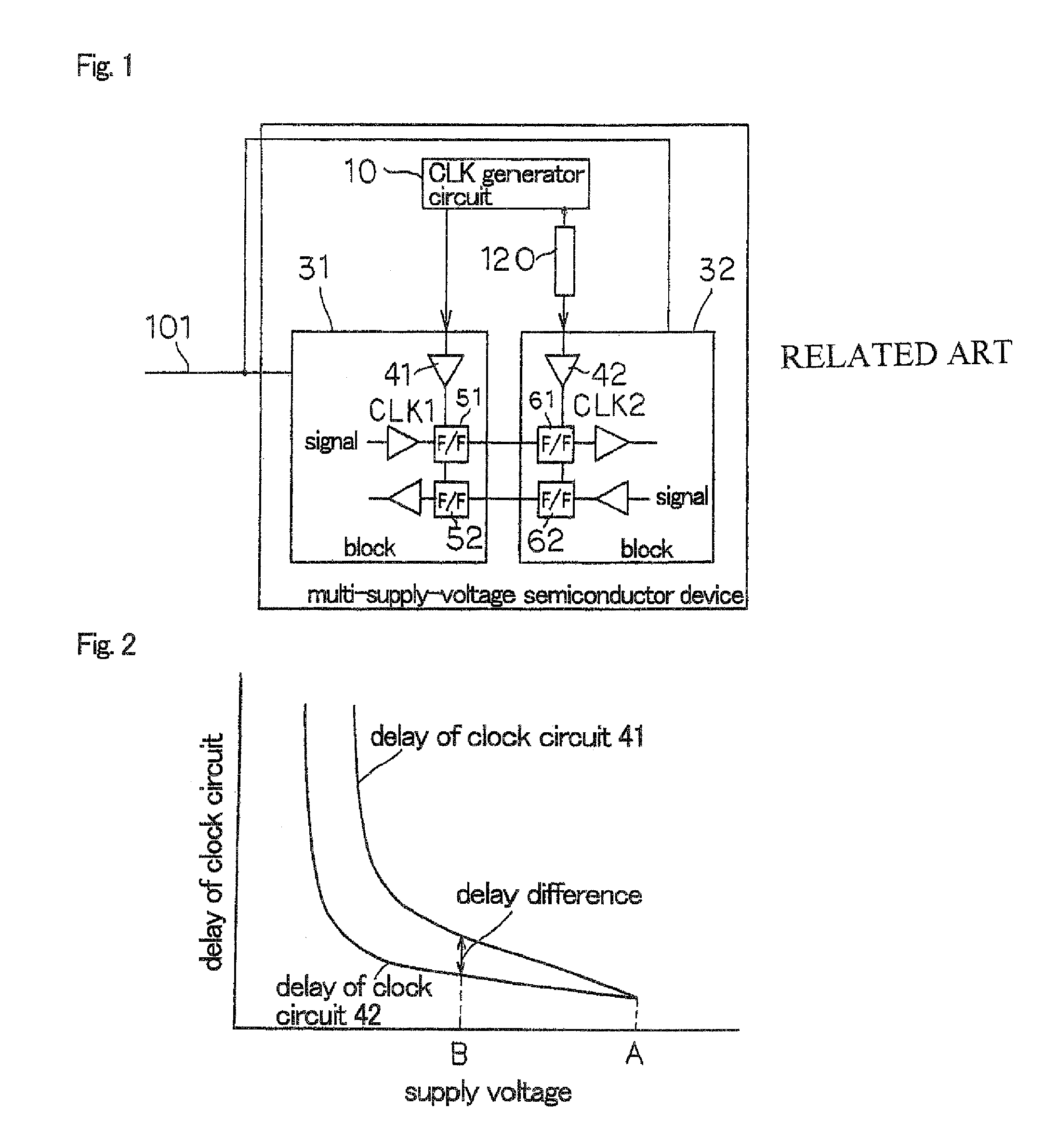
[0101]FIG. 6 is a block diagram showing a configuration of a multi-supply-voltage semiconductor device according to a first embodiment of the present invention. Components in FIG. 6 that are the same as those in FIG. 1 are labeled the same reference numerals, the description of which will be omitted.

[0102]A multi-supply-voltage semiconductor device according to the first embodiment includes clock (CLK) generator circuit 10, blocks 31, 32, and variable delay circuit 20. The multi-supply-voltage semiconductor device of the first embodiment has a configuration in which delay circuit 120 of the multi-supply-voltage semiconductor device shown in FIG. 1 is replaced with variable delay circuit 20.

[0103]Inputted into the multi-supply-voltage semiconductor device of the first embodiment is variable power supply 101 the power supply voltage of which changes. Variable power supply 101 is supplied to variable delay circuit 20 as well as to blocks 31, 32. If variable power supply 101 is the only...

second embodiment

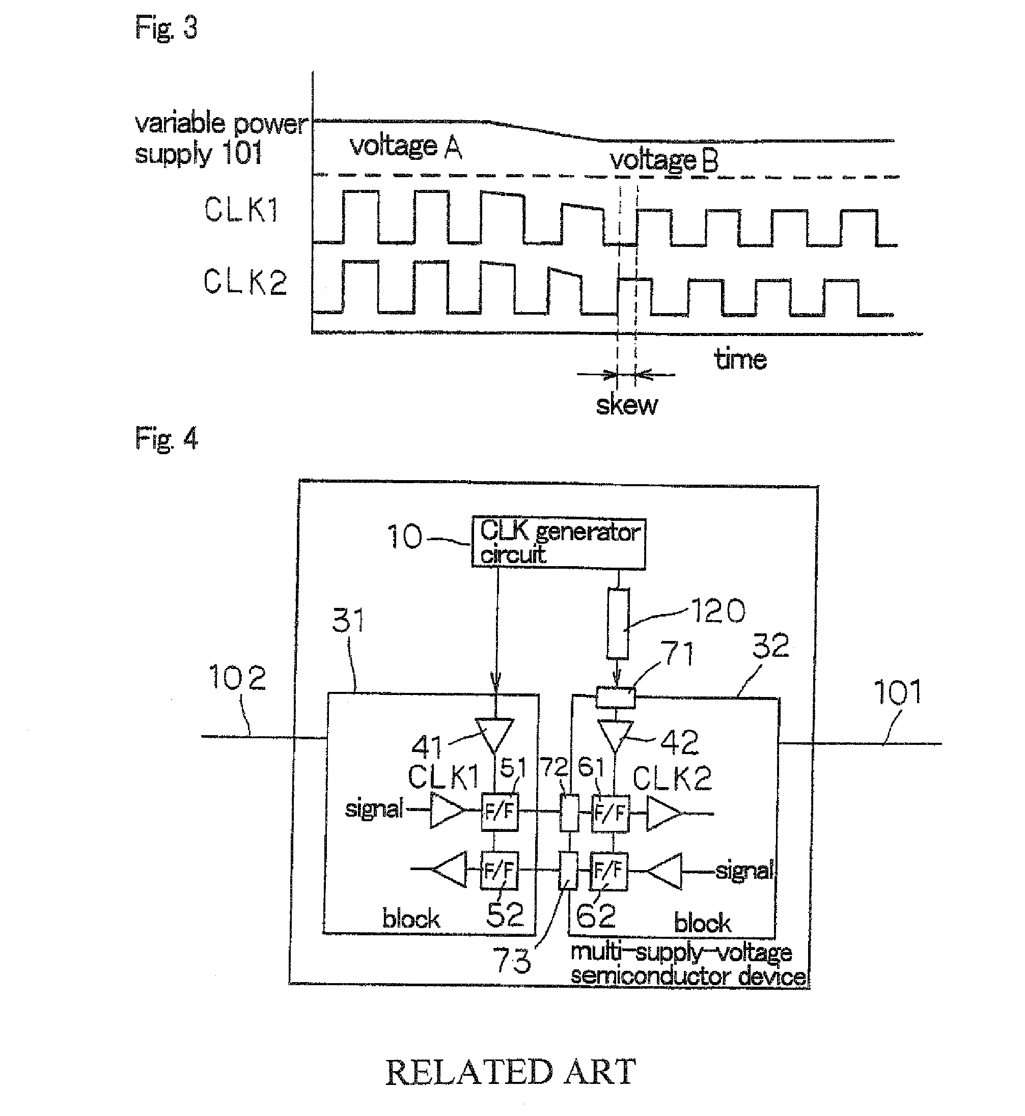
[0118]A multi-supply-voltage semiconductor device according to a second embodiment of the present invention will be described below. FIG. 12 is a block diagram showing a configuration of a multi-supply-voltage semiconductor device according to the second embodiment of the present invention. Components in FIG. 12 that are the same as those in FIG. 6 are labeled the same reference numerals, the description of which will be omitted.

[0119]While the multi-supply-voltage semiconductor device in the first embodiment of the present invention descried above has a variable delay circuit provided in one of its blocks, the multi-supply-voltage semiconductor device in the second embodiment of the present invention has variable delay circuits provided in multiple or in all blocks as shown in FIG. 12.

[0120]If clock circuit 41 is formed by high-threshold transistors and clock circuit 42 is formed by low-threshold transistors, variable delay circuit 20 will be formed by high-threshold transistors as...

third embodiment

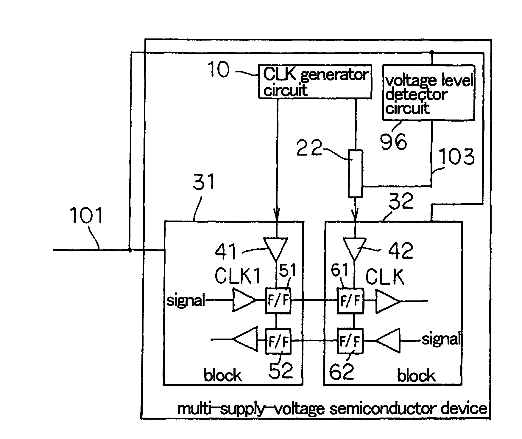
[0123]A multi-supply-voltage semiconductor device according to a third embodiment of the present invention will be described below. In the first and second embodiments described above, variable delay circuit 20 is provided to reduce clock skew due to a change in voltage of variable power supply 101 to stabilize operation of the blocks. However, a malfunction can occur if changes in delays of variable delay circuit 20 and clock circuits 41, 42 go out of synchronization while the voltage of variable power supply 101 is changing. The multi-supply-voltage semiconductor device of the third embodiment stops a clock signal supplied from clock generator circuit 10 during a change in the power supply voltage in order to stabilize operation of the blocks.

[0124]The multi-supply-voltage semiconductor device of the third embodiment further includes voltage change detector circuit 90 and AND circuits 91, 92, as shown in FIG. 13, in addition to the components of the multi-supply-voltage semiconduc...


PUM


Abstract

In a multi-supply-voltage semiconductor device including multiple blocks each of which has independent clock circuit, and operating with variable power supply, variable delay circuit which changes the amount of delay in accordance with the voltage value of the variable power supply is provided to a clock signal supplied to several blocks from clock generator circuit. This can reduce clock skew between the blocks even when the power supply voltage of variable power supply is changed.

Description

[0001]This application claims priority from PCT Application No. PCT / JP2004 / 010096 filed Jul. 15, 2004 and from Japanese Application No. 2003-277563 filed Jul. 22, 2003, which applications are incorporated herein by reference.TECHNICAL FIELD[0002]The present invention relates to a multi-supply-voltage semiconductor device operation with multiple power supply voltages and, in particular, to a multi-supply-voltage semiconductor device consisting of multiple blocks, some or all of which have independent clock circuits.BACKGROUND ART[0003]Electronic equipment such as mobile phones containing semiconductor devices has been reduced in size and power consumption in recent years. Accordingly, there is a demand for reduction in power consumption in semiconductor devices.[0004]It is effective for reducing power consumption to decrease power supply voltages. Decreasing power supply voltages also decreases leakage current, which results in reduction in power consumption. However, decreasing powe...

Claims


Application Information

Patent Timeline
Patent Type & Authority Patents(United States)
IPC IPC(8): H03K3/00G06F1/10G06F1/32H01L21/82H01L27/04H03K5/00H03K5/13H03K5/135H03K19/0185
CPCG06F1/10G06F1/3203G06F1/324G06F1/3296H03K5/133H03K5/135H03K2005/00032H03K2005/00045H03K2005/0013Y02B60/1217Y02B60/1285Y02D10/00
Inventor NOMURA, MASAHIRO
Owner NEC CORP
Why Eureka
Try Eureka