
Method and apparatus for reducing clock skew in an integrated circuit

a technology of integrated circuits and clocks, applied in the direction of instruments, digital transmission, generating/distributing signals, etc., can solve the problems of difficult to achieve a reliable performance, data may no longer be valid, and significant skew between these clocks, so as to reduce clock skew

Inactive Publication Date: 2005-10-25
SILICON INTEGRATED SYSTEMS
View PDF7 Cites 11 Cited by
  • Summary
  • Abstract
  • Description
  • Claims
  • Application Information

AI Technical Summary

Benefits of technology

The present invention provides a method and apparatus for reducing clock skew in an integrated circuit chip working in synchronous operation mode. This is achieved by providing a first source clock and a second source clock for a first circuit block and a second circuit block, respectively. An operation mode signal is set to synchronize the second circuit block with the first circuit block, and the clock input terminal of the second circuit block is switched when the second circuit block is configured to operate in synchronization with the first circuit block. This ensures that both circuit blocks operate in accordance with the same first source clock. The invention also includes a first multiplexer and a second multiplexer with substantially the same architecture, such that a signal of the first source clock, propagated by the first and the second multiplexers respectively, has substantially the same delay. The technical effect of the invention is to reduce clock skew and improve synchronous operation mode in an integrated circuit chip.

Problems solved by technology

However, since the latency of a typical synchronizer is one or two cycles depending on the relationship between the source and the destination clock domains, it is difficult to attain a reliable performance.
Hence, there is a considerable skew between these clocks.
Nevertheless, as the clock rates of computer systems increase dramatically, the data may no longer be valid if there are clock skews within the IC chips and systems.

Method used


Image

  • Method and apparatus for reducing clock skew in an integrated circuit
  • Method and apparatus for reducing clock skew in an integrated circuit
  • Method and apparatus for reducing clock skew in an integrated circuit

Examples


Embodiment Construction

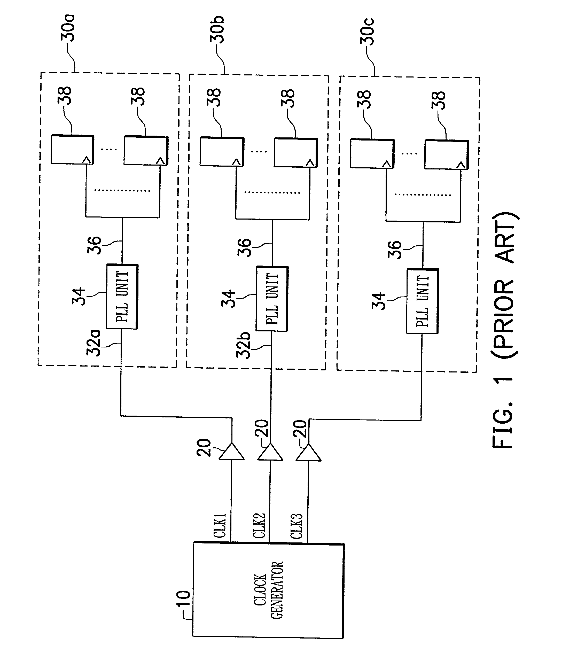
[0016]Analyzing from an exemplary clock input circuit of an IC chip in accordance with prior art in FIG. 1, the clock skew between flip-flops 38 of circuit blocks 30a and 30b includes three factors: the inaccuracy of PLL unit 34 of circuit block 30a, the inaccuracy of PLL unit 34 of circuit block 30b, and clock skew between CLK1 and CLK2 of clock generator 10. The present invention is directed to the clock skew caused by different source clocks, therefore, the present invention discloses a scheme that dynamically switches source clocks, instead of applying fixed source clocks, to different circuit blocks.

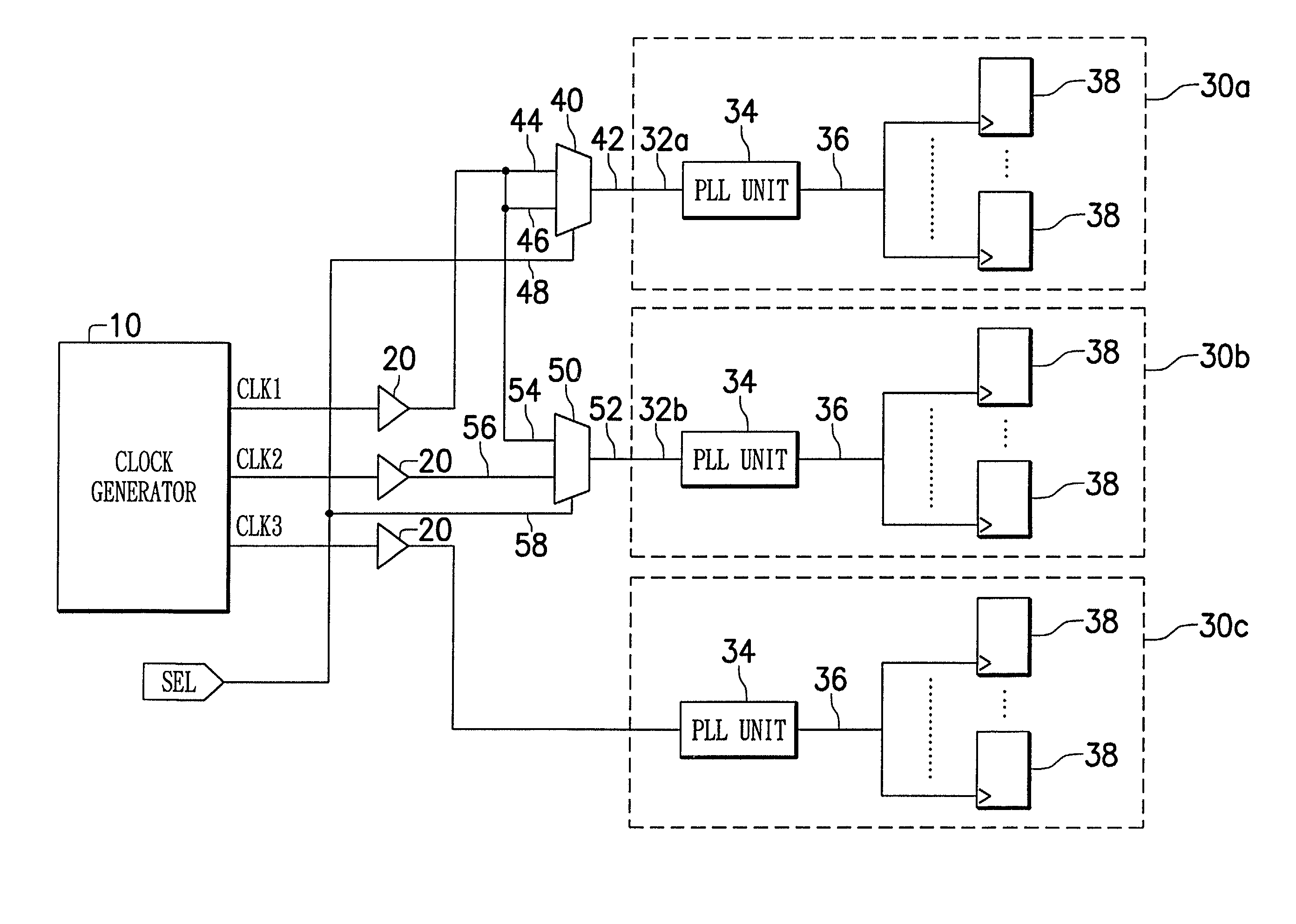
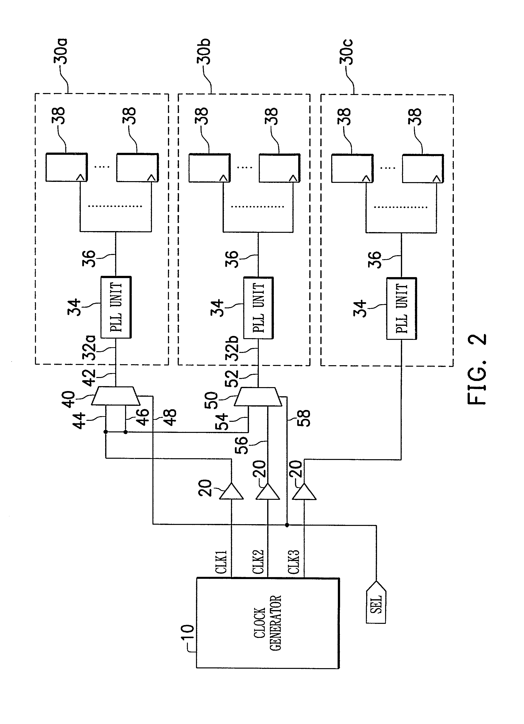
[0017]FIG. 2 is a block diagram that illustrates a preferred clock input circuit of an IC chip in accordance with the present invention. It is understood that components shown in FIG. 2 are similar to components shown in FIG. 1, and are identified by the same reference numbers. According to the present invention, one multiplexer 40 is added between circuit block 30a and the source c...


PUM


Abstract

A method is provided to reduce clock skew in an integrated circuit having a number of circuit blocks, which comprises the following steps. A first source clock coupled to a clock input terminal of a first circuit block within the circuit blocks is provided, as is a second source clock coupled to a clock input terminal of a second circuit block within the circuit blocks. When the second circuit block is configured to operate in synchronization with the first circuit block, the clock input terminal of the second circuit block is switched to the first source clock, and thus both the first circuit block and the second circuit block can operate in accordance with the same first source clock.

Description

FIELD OF THE INVENTION[0001]The present invention relates generally to the operation of integrated circuits and, in particular, to a method and apparatus for reducing clock skew between different circuit blocks of an integrated circuit.BACKGROUND OF THE INVENTION[0002]In modern integrated circuit (IC) chip designs, multiple clocks may be desired or required in order to provide various operating clock rates within an IC chip. Allowing the IC chip to operate at various operating clock rates can achieve better performance and compatibility while working with a variety of peripheral devices. A typical personal computer chipset provides at least four types of clock inputs, for example, CPU clock, DRAM clock, PCI clock, and AGP clock, to control the respective circuit blocks. These clocks allow the chipset to communicate with host bus, DRAM bus, PCI bus, AGP bus, and others. Moreover, depending on their functionality, each bus can work at different clock rates to achieve better performanc...

Claims


Application Information

Patent Timeline
Patent Type & Authority Patents(United States)
IPC IPC(8): G06F1/10
CPCG06F1/10
Inventor CHEN, CHIEN-MINGLEE, MING-HSIEN
Owner SILICON INTEGRATED SYSTEMS
Learn More