Power lead-on-chip ball grid array package

a power lead and chip technology, applied in the field of semiconductor devices, can solve the problems of inability to connect the number of signal and power lines required by today's devices, the conventional approach to electrically connecting signals and power to the integrated circuit die, and the design and packaging of significant challenges of these devices

Active Publication Date: 2012-03-06
NXP USA INC
View PDF21 Cites 3 Cited by
  • Summary
  • Abstract
  • Description
  • Claims
  • Application Information

AI Technical Summary

Problems solved by technology

As the density and complexity of integrated circuit devices increases and the size of such devices shrinks, significant challenges are posed in the design and packaging of these devices.
One challenge is that more and more power and signal lines must be electrically connected to the integrated circuit die as the circuit complexity increases, though there is less and less space to allow for such connection as the device sizes shrink.
Another challenge is that the conventional approaches for electrically connecting signal and power to the integrated circuit die—such as bonding lead-on-chip (LOC) or tape automated bonding (TAB) leadframe conductors to the die area—are simply not a viable solution for connecting the number of signal and power lines required by today's devices, given the relatively large and unwieldy size of such conductors in comparison to the die size.
Such conventional approaches also present packaging challenges in protecting the integrated circuit die from structural or mechanical damage, such as can be caused by moisture or other environmental exposure when leadframe conductors extend through the protective packaging in order to make electrical contact to the outside world.
However, these wirebond packaging solutions very often deliver power unevenly to the entire die since the power lines are wirebonded to peripheral bonding pads arrayed on all sides of the active or face surface 23 of the die 22, as illustrated in FIGS. 1 and 2.
The problem of power loss can be especially acute with low power devices using conventional wirebond packaging.
For example, with products in the 5-8 watt range, every milli-volt of voltage degradation over the area of a particular power domain can result in performance and / or yield loss.
Such voltage drops can impair the performance of high speed CMOS digital logic (e.g., above 600 Mhz) located in areas that are more than approximately 2 mm from a package level supply terminal.
Though flip-chip packaging can provide excellent power distribution, its costs are usually higher than wire bond packages and can limit its application space.

Method used


Image

  • Power lead-on-chip ball grid array package
  • Power lead-on-chip ball grid array package
  • Power lead-on-chip ball grid array package

Examples


Embodiment Construction

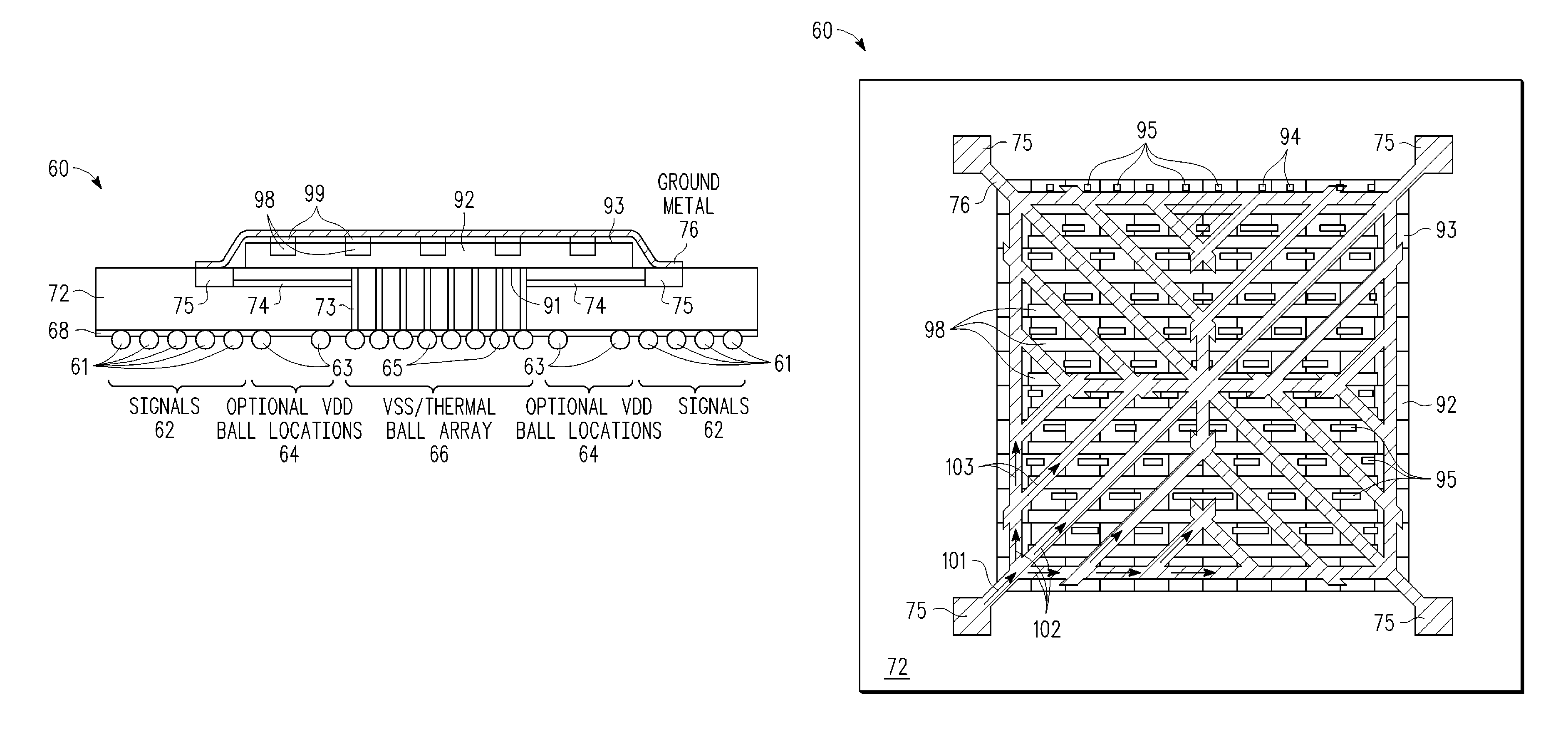
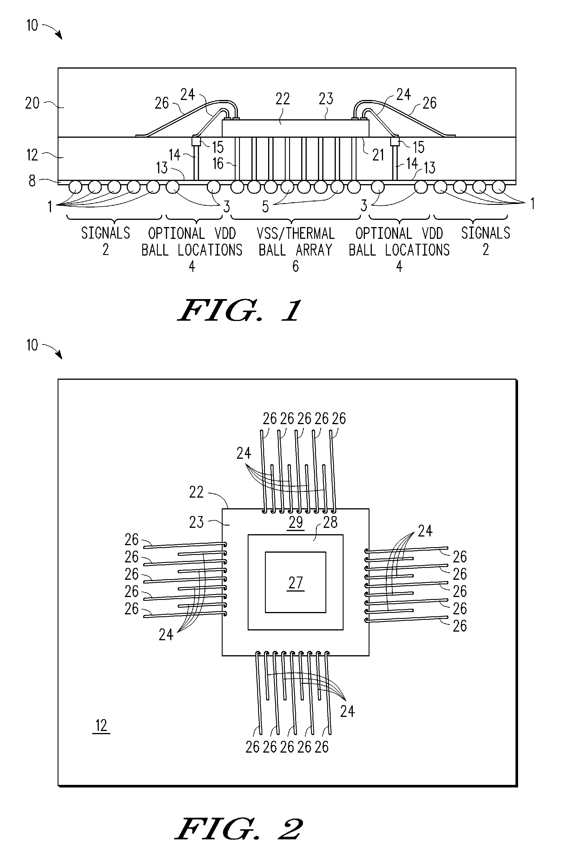
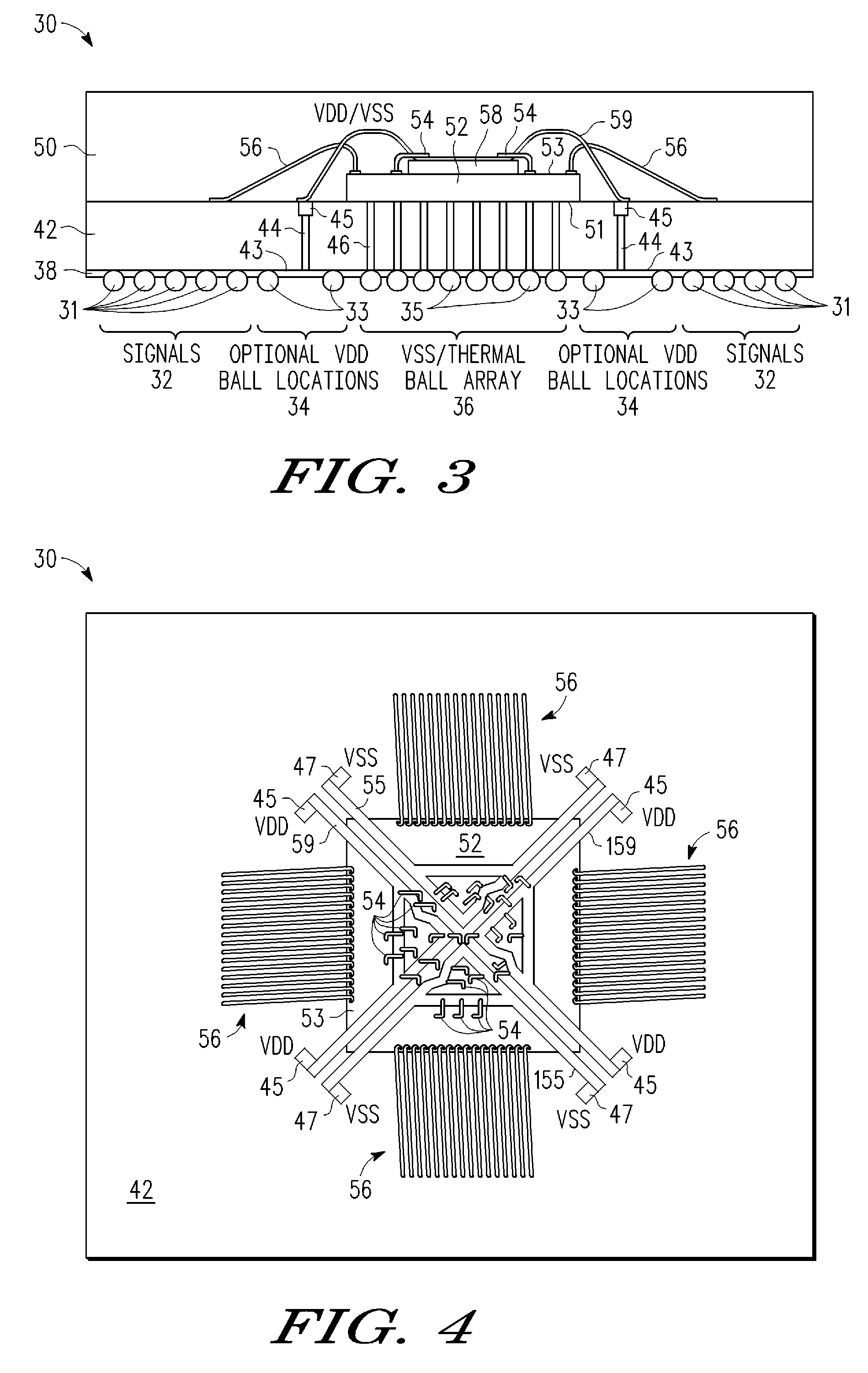
[0018]A method and apparatus are described for encapsulating a semiconductor die in a package in which an encapsulated leadframe structure is bonded and connected to an integrated circuit die so as to distribute power and / or ground to die level bond pads distributed across the die area. In addition to improving power distribution across the die area, the encapsulated leadframe structure also provides additional contact areas at the periphery of the die for wirebonded signal lines. The leadframe structure is electrically connected to an off-chip power and / or ground supply through electrically conductive paths formed in a carrier substrate (e.g., solder balls, conductive traces, vias, contact pads). In addition, the leadframe structure is formed from one or more patterned conductor layers that are disposed over the integrated circuit die area to make electrical contact with an array of power and / or ground supply terminals in the integrated circuit die. To distribute power across the d...


PUM


Abstract

A packaging assembly (30), such as a ball grid array package, is formed which distributes power across an interior region of an integrated circuit die (52) by using an encapsulated patterned leadframe conductor (59) that is disposed over the die (52) and bonded to a plurality of bonding pads (45) formed in a BGA carrier substrate (42) and in the interior die region, thereby electrically coupling the interior die region to an externally provided reference voltage.

Description

BACKGROUND OF THE INVENTION[0001]1. Field of the Invention[0002]The present invention is directed in general to the field of semiconductor devices. In one aspect, the present invention relates to electronic component packaging.[0003]2. Description of the Related Art[0004]As the density and complexity of integrated circuit devices increases and the size of such devices shrinks, significant challenges are posed in the design and packaging of these devices. One challenge is that more and more power and signal lines must be electrically connected to the integrated circuit die as the circuit complexity increases, though there is less and less space to allow for such connection as the device sizes shrink. Another challenge is that the conventional approaches for electrically connecting signal and power to the integrated circuit die—such as bonding lead-on-chip (LOC) or tape automated bonding (TAB) leadframe conductors to the die area—are simply not a viable solution for connecting the num...

Claims


Application Information

Patent Timeline
Patent Type & Authority Patents(United States)
IPC IPC(8): H01L21/44
CPCH01L23/3128H01L23/49816H01L23/49833H01L23/50H01L24/49H01L24/73H01L24/85H01L24/91H01L23/4951H01L2924/07802H01L2924/014H01L2924/01023H01L2924/00014H01L24/48H01L2924/15311H01L2924/15192H01L2924/15184H01L2924/14H01L2924/09701H01L2924/01082H01L2924/01079H01L2924/0105H01L2924/01047H01L2924/01033H01L2924/01029H01L2924/01015H01L2924/01014H01L2224/85205H01L2224/85201H01L2224/85191H01L2224/4945H01L2224/24226H01L2224/32145H01L2224/48091H01L2224/48145H01L2224/48227H01L2224/48235H01L2224/48471H01L2224/49175H01L2224/49433H01L2224/78H01L2924/00H01L2924/181H01L2224/85203H01L2224/45099H01L2224/05599H01L2924/00012H01L2224/4554
Inventor JOHNSTON, JAMES P.LEE, CHU-CHUNGTRAN, TU-ANH N.MILLER, JAMES W.HESS, KEVIN J.
Owner NXP USA INC
Why Eureka
Try Eureka