Thin smart card module having strap on carrier

a smart card and carrier technology, applied in the field of smart card structure and method, can solve the problems of mechanical weakness of modules and expose the chips to the risk of breakage, and achieve the effects of reducing module thickness, enhancing module robustness, and improving mechanical robustness and environmental insensitivity

Active Publication Date: 2012-03-27
TEXAS INSTR INC
View PDF8 Cites 24 Cited by
  • Summary
  • Abstract
  • Description
  • Claims
  • Application Information

AI Technical Summary

Benefits of technology

[0007]Applicants recognize the need for a paradigm shift in assembling and packaging semiconductor chips in Smart Card modules in order to gain the benefit of reduced module thickness while, at the same time, improving mechanical robustness and environmental insensitivity. Applicants have further shown in detailed investigations that, when properly formed, sturdy metals can not only dramatically enhance module robustness while reducing thickness, but also provide opportunity for reducing manufacturing cost and enhancing stacking and combinatory assembly of different modules for new applications.
[0009]With this solution, the overall module thickness can be kept to less than 250 μm without dangerously thinning the chip (to less than 200 μm). The sturdy carrier increases the bending / flexure reliability of the module, and additional strength can be gained by filling any remaining gap between chip and carrier with molding compound. The metallic carrier further provides contact areas for higher level system interconnection by the customer (stacking of modules, stacking of chips). The flip-assembled chip further offers opportunities for attachment of heat sinks and thus very effective device cooling.

Problems solved by technology

The foils in turn, render the module mechanically weak and expose the chip to the risk of breakage.

Method used


Image

  • Thin smart card module having strap on carrier
  • Thin smart card module having strap on carrier
  • Thin smart card module having strap on carrier

Examples


Embodiment Construction

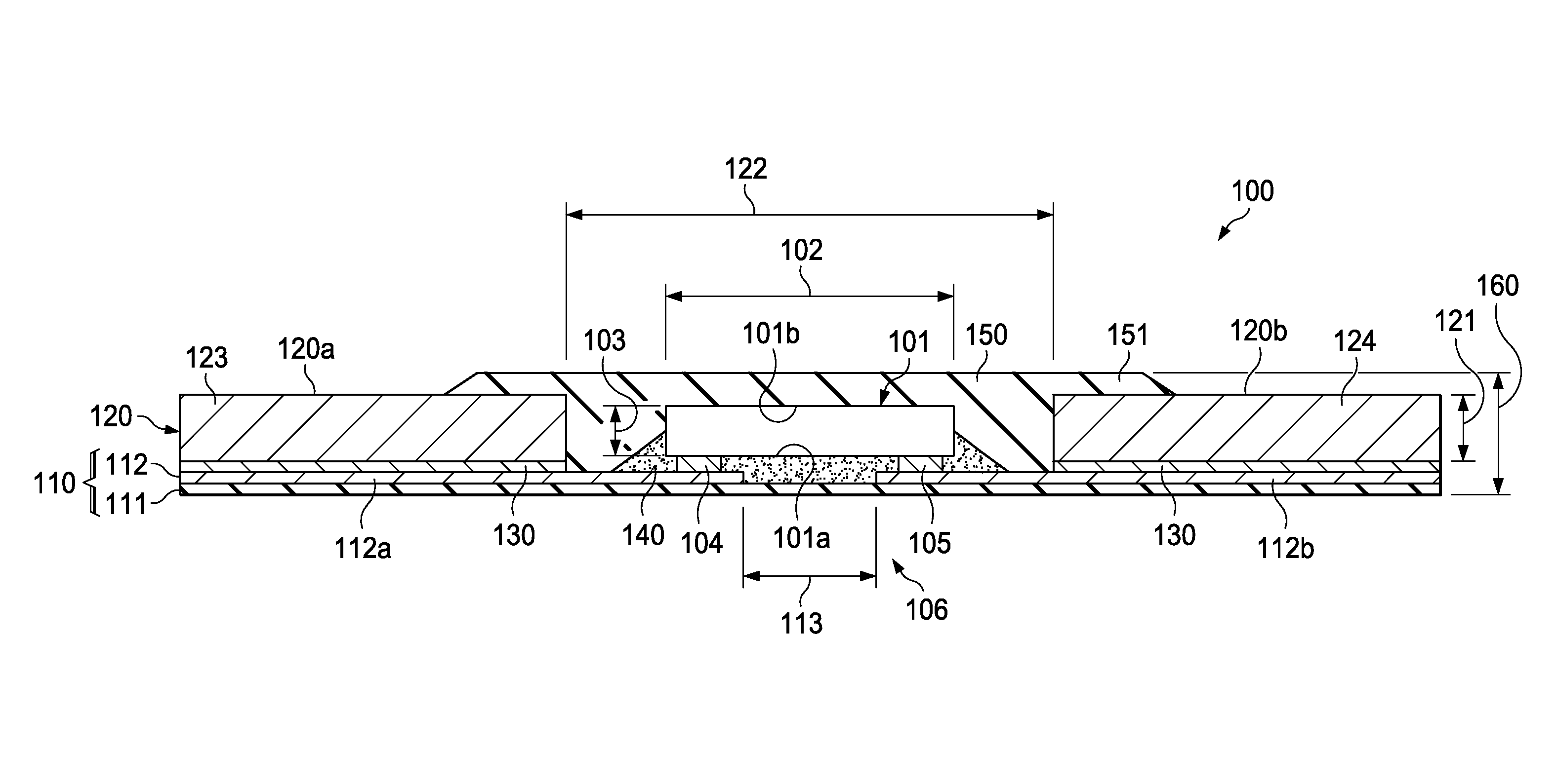
[0023]A Smart Card module according to the embodiments of the invention includes a conductive elongated flat carrier structured as two portions surrounding a recess; the carrier material has a first thickness. A semiconductor chip of a second thickness is in the recess and has electrical connections of a height to the carrier portions. The sum of the second thickness and the connection height is approximately equal to the first thickness. Encapsulation compound fills the space of the recess not occupied by the chip.

[0024]With reference now to the figures and in particular with reference to FIG. 1, an embodiment of the invention is a Smart Card Module, generally designated 100 in FIG. 1, which includes a semiconductor chip 101. In other embodiments, two or more chips, or stacks of chips may be employed. Chip 101 has a first length 102, a first thickness 103, and metallic contact bumps of a height 106. The bumps are attached to chip surface 101a and are preferably grouped in sets loca...


PUM

PropertyMeasurementUnit
thicknessaaaaaaaaaa
lengthaaaaaaaaaa
thicknessaaaaaaaaaa

Abstract

A Smart Card module with flip-assembled chip (101) on a metallic strap (112) adhering to an insulating substrate (111). Chip (101) is in the gap (122) of a metal carrier (120), strap (112) conductively attached to the carrier. Carrier (120) is designed to practically surround the chip, and has a thickness about equal to the chip thickness. Overall module thickness is less than 250 μm without dangerously thinning the chip. Additional strength may be acquired by filling any space of gap (122) not occupied by chip (101) with encapsulation compound (150). Metal carrier (120) further provides contact areas (120a, 120b) for higher level system interconnection (stacking of modules).

Description

FIELD[0001]Embodiments of the invention are related in general to the field of electronic systems and semiconductor devices and more specifically to structure and method of a Smart Card, which combines thinness with robustness and thus exhibits high reliability and offers widespread applications.DESCRIPTION OF RELATED ART[0002]The Smart Card consists of one or more integrated circuit chips encapsulated in a convenient form to be carried on one's person. The encapsulation may be a bank card, a tag, a key, or a mobile telephone; it may have almost any shape, size and thickness that is convenient for the user to carry, insert, or connect into a device and retrieve. A number of industries produce the diversified Smart Card encapsulations, while the semiconductor industry supplies the modules, in which the semiconductor chips are assembled and packaged.[0003]Driven by wider diversification, Smart Card modules face a relentless application pressure for reducing thickness and overall size,...

Claims


Application Information

Patent Timeline
Patent Type & Authority Patents(United States)
IPC IPC(8): G06K19/06
CPCG06K19/07718G06K19/07743H01L2224/16225Y10T29/49117H01L2924/01327H01L2924/00
Inventor BHANDARKAR, SARVOTHAMHOANG, HOANG
Owner TEXAS INSTR INC
Why Eureka
Try Eureka