

Polishing method with inert gas injection
a technology of inert gas and polishing method, which is applied in the direction of manufacturing tools, other chemical processes, chemistry apparatus and processes, etc., can solve the problems of uneven surface topography, inability to extend the polish time indefinitely, and difficulty in uniform polishing
- Summary
- Abstract
- Description
- Claims
- Application Information
AI Technical Summary
Benefits of technology
Problems solved by technology
Method used
Image

Examples
Embodiment Construction
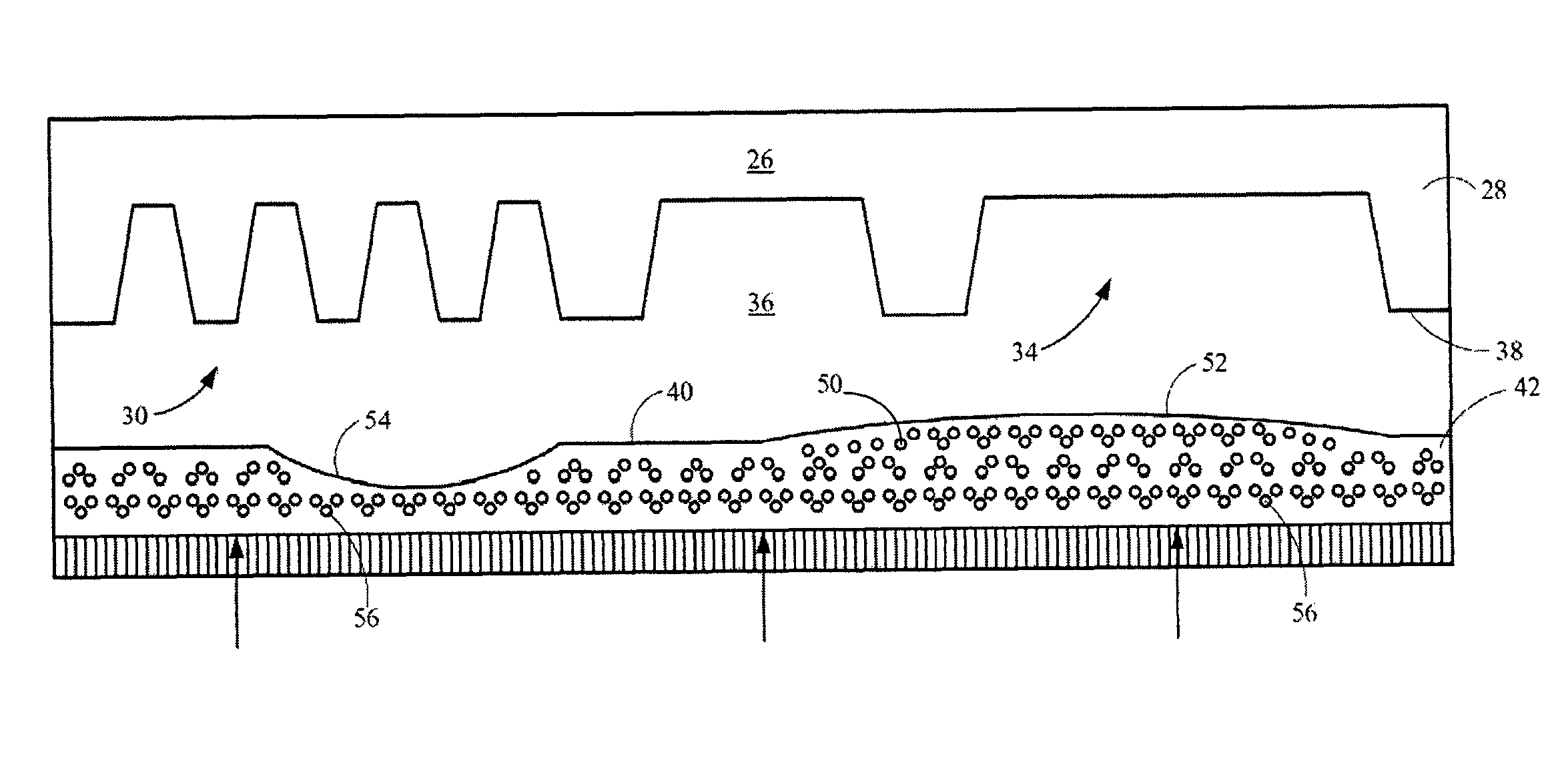
[0016]Shown in FIG. 1, in cross-section, is a substrate 10 having been polished by a prior art polishing process. Substrate 10 includes an inlay pattern formed in a dielectric layer 12. The inlay pattern is formed by etching recessed features into insulating layer 12 using a lithographic masking and etching process. Metal interconnects are formed in insulating layer 12 by depositing a metal layer onto substrate 10 that fills the recessed regions in insulating 12 and overlies remaining portions of the substrate 10. In accordance with the prior art, a CMP process is carried out to remove portions of the metal layer from a principal surface 14 of insulating layer 12. Upon completion of the CMP process, metal regions 16 remain in the recesses in insulating layer 12.
[0017]As shown in FIG. 1, the CMP process of the prior art forms an uneven upper surface across substrate 10. In particular, relative to principal surface 14, the surface profile varies in relation to the overall dimensions a...
PUM
| Property | Measurement | Unit |
|---|---|---|
| feature density | aaaaa | aaaaa |
| concentration | aaaaa | aaaaa |
| size | aaaaa | aaaaa |
Abstract
Description
Claims
Application Information