Semiconductor integrated circuit device having a dummy metal wiring line

a technology of integrated circuits and metal wire lines, which is applied in the direction of semiconductor devices, semiconductor/solid-state device details, electrical equipment, etc., can solve the problems of wire breakage, the proximity effect degrades the dimensional precision of wiring,

Active Publication Date: 2012-04-17
SOCIONEXT INC
View PDF14 Cites 25 Cited by
  • Summary
  • Abstract
  • Description
  • Claims
  • Application Information

AI Technical Summary

Benefits of technology

[0011]In accordance with the present invention, the metal wiring line is placed in the boundary portion between the first and second adjacent cells so as not to short-circuit the power supply line and the ground line. Accordingly, before a cell is placed, a distance to a proximate line from the intra-cell line closest to the boundary portion is determined within the cell. Therefore, it is possible to predict the magnitude of variation in line width due to the optical proximity effect, and perform OPC correction with respect to standard cells before cell placement. As a result, the OPC correction after cell placement is no more necessary. This allows reductions in the amount of data for OPC correction and OPC process time, and also allows a reduction in the number of development steps.
[0012]Thus, in accordance with the present invention, it is possible to prevent the thinning of the metal wiring line closest to the cell boundary, and wire breakage therein without involving increases in the amount of data for OPC correction and OPC process time.

Problems solved by technology

The optical proximity effect degrades the dimensional precision of wiring.
Accordingly, depending on a line-to-line space, the line width is reduced to a value smaller than a specified value under the influence of the optical proximity effect and, in some cases, may result in wire breakage.

Method used


Image

  • Semiconductor integrated circuit device having a dummy metal wiring line
  • Semiconductor integrated circuit device having a dummy metal wiring line
  • Semiconductor integrated circuit device having a dummy metal wiring line

Examples


embodiment 1

(Embodiment 1)

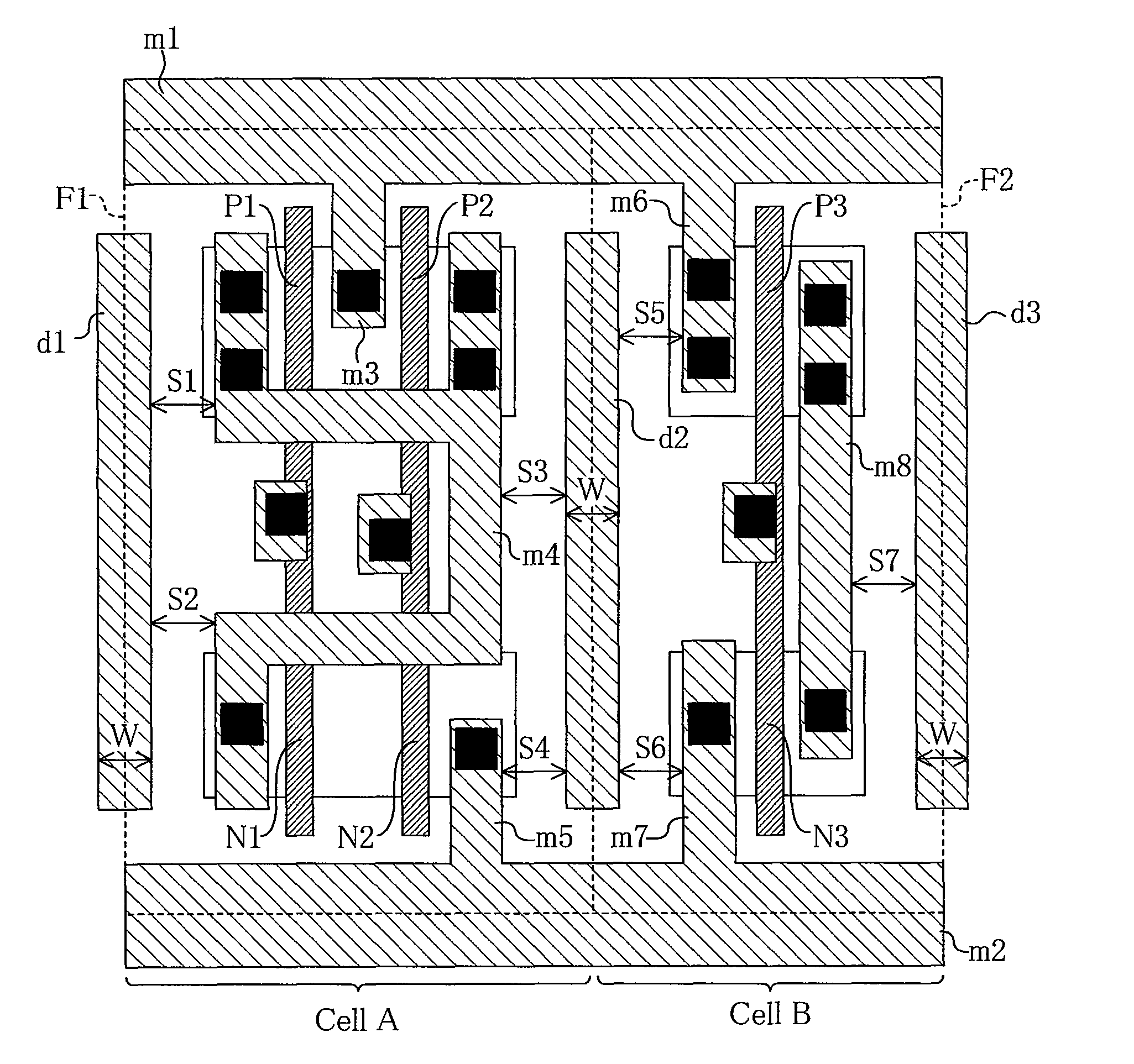
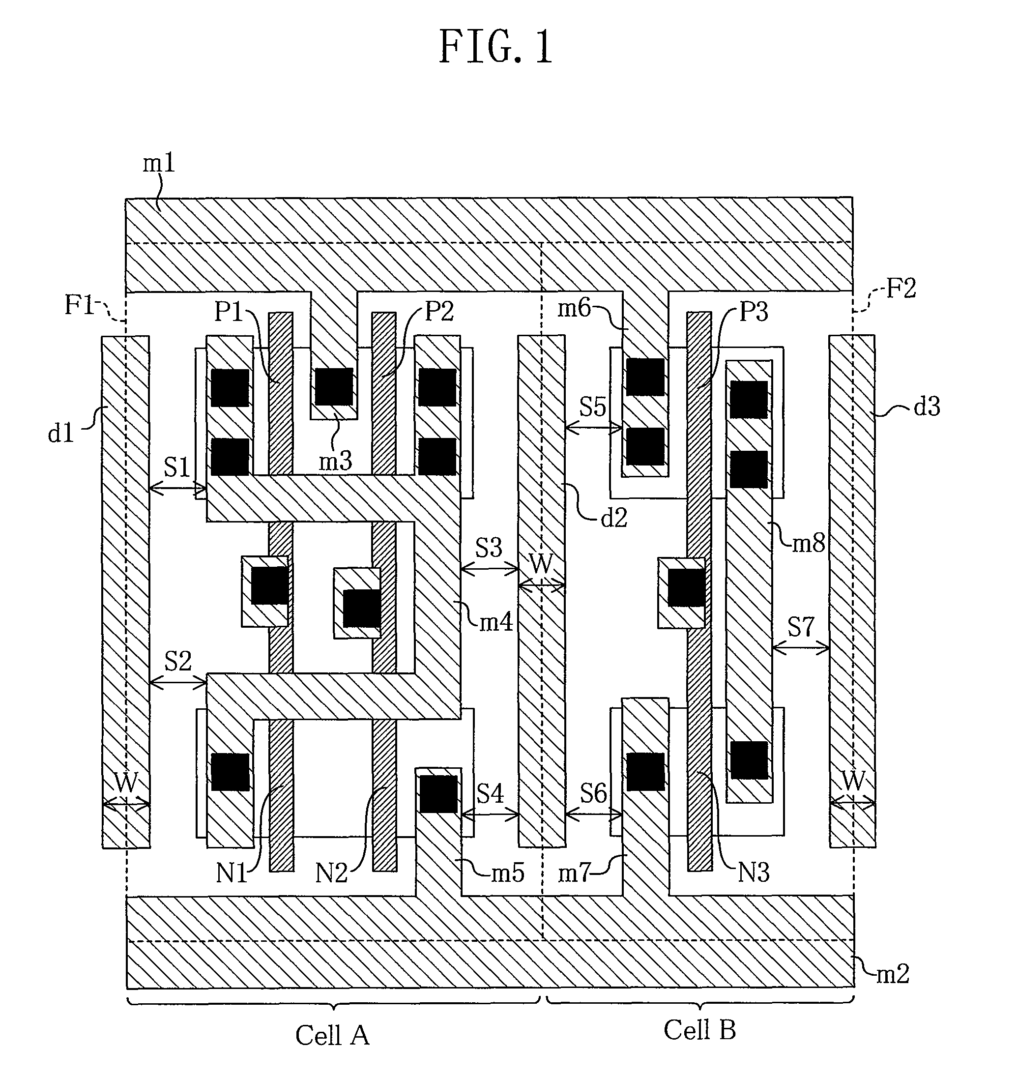
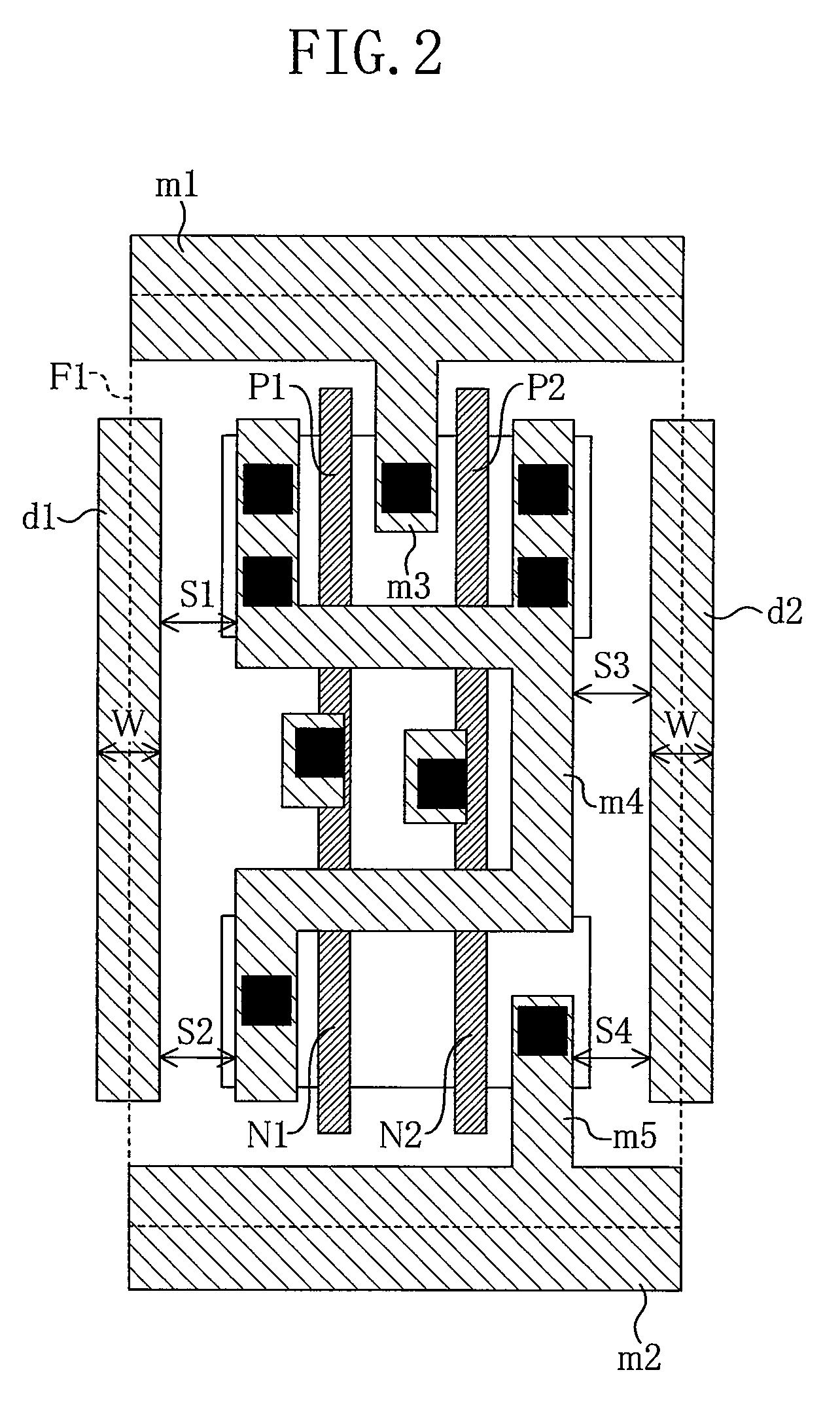
[0046]FIG. 1 is a layout plan view showing a structure of a semiconductor integrated circuit device according to a first embodiment. In FIG. 1, a power supply line m1 and a ground line m2 are placed to extend in a first direction (transverse direction in the drawing). In the region interposed between the power supply line m1 and the ground line m2, a cell A as a first cell and a cell B as a second cell are placed to be adjacent to each other in the first direction.

[0047]Each of the cells A and B has a transistor and an intra-cell line each for implementing a circuit function. In this structure, the cell A forms a 2-input NAND gate, and the cell B forms an inverter.

[0048]That is, in the cell A, PMOS transistors P1 and P2 and NMOS transistors N1 and N2 are disposed. The PMOS transistors P1 and P2 have a shared source, to which a power supply voltage is supplied via a metal wiring line m3 extracted from the power supply line m1. On the other hand, the PMOS transistors P1 ...

embodiment 2

(Embodiment 2)

[0060]FIG. 7 is a layout plan view showing a structure of a semiconductor integrated circuit device according to a second embodiment. In FIG. 7, the structures of the power supply line m1, the ground line m2, and the cells A and B are the same as in FIG. 1. Components common to those shown in FIG. 1 are provided with the same reference numerals as used in FIG. 1, and a detailed description thereof is omitted herein.

[0061]In the structure of FIG. 7, metal wiring lines d8 and d9 each extending in the second direction (vertical direction in the drawing) orthogonal to the first direction are placed so as not to short-circuit the power supply line m1 and the ground line m2. That is, the metal wiring line d8 as the first line is formed to protrude from the power supply line m1, while the metal wiring line d9 as the second line is formed to protrude from the ground line m2. The metal wiring lines d8 and d9 are not connected to each other. The metal wiring lines d8 and d9 are ...

embodiment 3

(Embodiment 3)

[0070]FIG. 11 is a layout plan view showing a structure of a semiconductor integrated circuit device according to a third embodiment. In FIG. 11, the structures of the power supply line m1, the ground line m2, and the cells A and B are the same as in FIG. 1. Components common to those shown in FIG. 1 are provided with the same reference numerals as used in FIG. 1, and a detailed description thereof is omitted herein.

[0071]In the structure of FIG. 11, a metal wiring line d22 extending in the second direction (vertical direction in the drawing) orthogonal to the first direction is placed so as not to short-circuit the power supply line m1 and the ground line m2. That is, the metal wiring line d22 is formed to protrude from the power supply line m1, and extend to the vicinity of the ground line m2, but is not connected to the ground line m2. The metal wiring line d22 is formed in the same wiring layer in which the power supply line m1, the ground line m2, and the intra-ce...


PUM


Abstract

There is provided a layout structure of a semiconductor integrated circuit capable of preventing the thinning of a metal wiring line close to a cell boundary and wire breakage therein without involving increases in the amount of data for OPC correction and OPC process time. In a region interposed between a power supply line and a ground line each placed to extend in a first direction, first and second cells each having a transistor and an intra-cell line each for implementing a circuit function are placed to be adjacent to each other in the first direction. In a boundary portion between the first and second cells, a metal wiring line extending in a second direction orthogonal to the first direction is placed so as not to short-circuit the power supply line and the ground line.

Description

RELATED APPLICATIONS[0001]This application is the U.S. National Phase under 35 U.S.C. §371 of International Application No. PCT / JP2009 / 000799, filed on Feb. 24, 2009, which in turn claims the benefit of Japanese Application No. 2008-176134, filed on Jul. 4, 2008, the disclosures of which Applications are incorporated by reference herein.TECHNICAL FIELD[0002]The present disclosure relates to a layout structure of a semiconductor integrated circuit which is effective in improving the dimensional precision of a wiring pattern.BACKGROUND ART[0003]As design rules have been increasingly reduced with miniaturization, variation in line width due to an optical proximity effect has become ignorable. The optical proximity effect is a phenomenon in which a finished value of a line width varies according to a distance to a proximate line. The optical proximity effect degrades the dimensional precision of wiring. Accordingly, depending on a line-to-line space, the line width is reduced to a value...

Claims


Application Information

Patent Timeline
Patent Type & Authority Patents(United States)
IPC IPC(8): H01L29/66H01L29/94H01L21/108
CPCH01L23/522H01L27/0207H01L27/11807H01L23/5286H01L2924/0002H01L2924/00
Inventor NISHIMURA, HIDETOSHISHIMBO, HIROYUKITOUBOU, TETSUROUTANIGUCHI, HIROKIYONEDA, HISAKO
Owner SOCIONEXT INC
Why Eureka
Try Eureka