Method for manufacturing electrophotographic photosensitive member
a photosensitive member and electrophotography technology, applied in the direction of electrographic process apparatus, instruments, corona discharge, etc., can solve the problems of difficult to reduce power consumption, difficult problem for conventional electrophotographic photosensitive member and electrophotographic apparatus, letter blur, etc., to reduce moisture adsorption, enhance hardness, and enhance abrasion resistance
- Summary
- Abstract
- Description
- Claims
- Application Information
AI Technical Summary
Benefits of technology
Problems solved by technology
Method used
Image
Examples
example 1
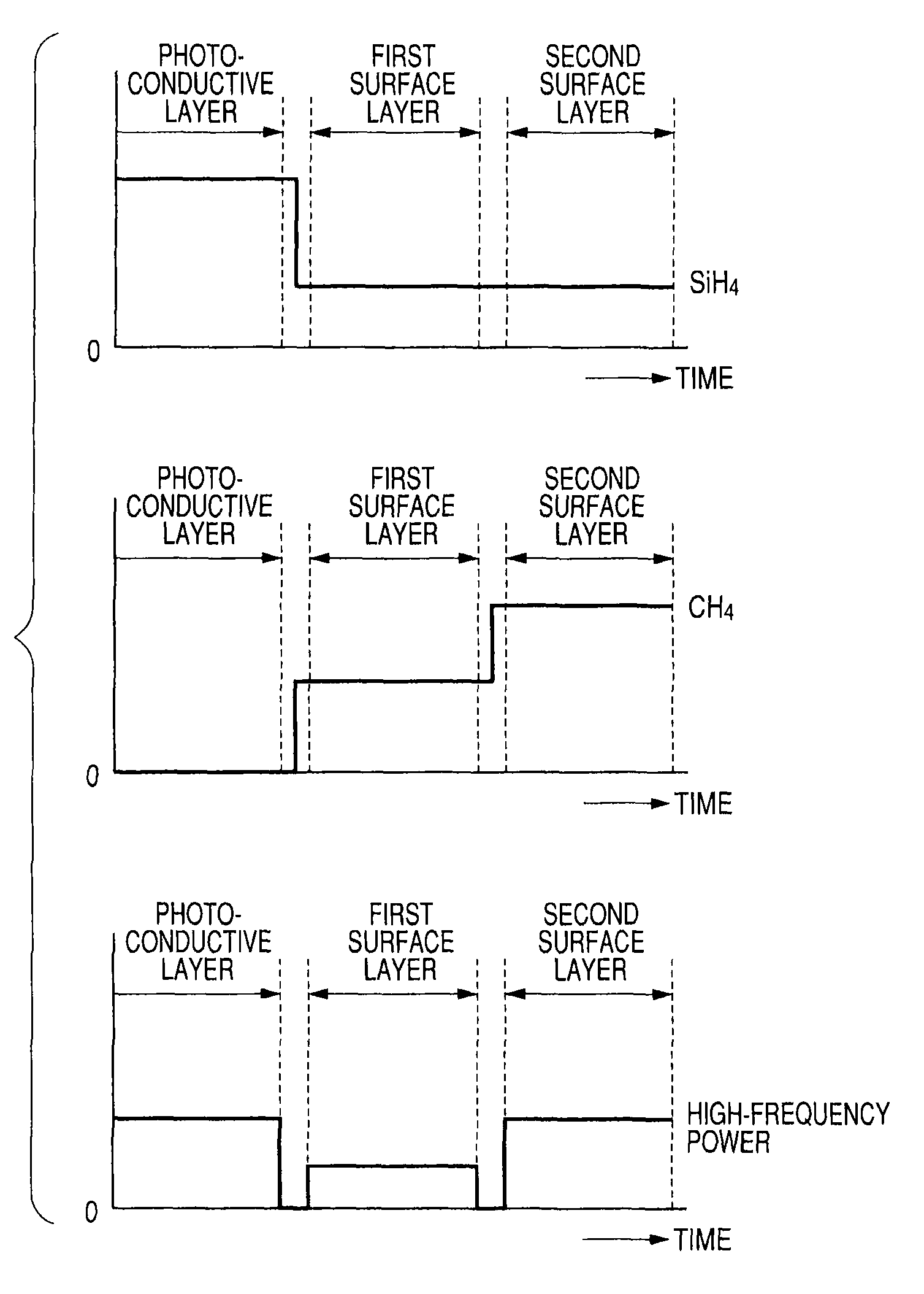
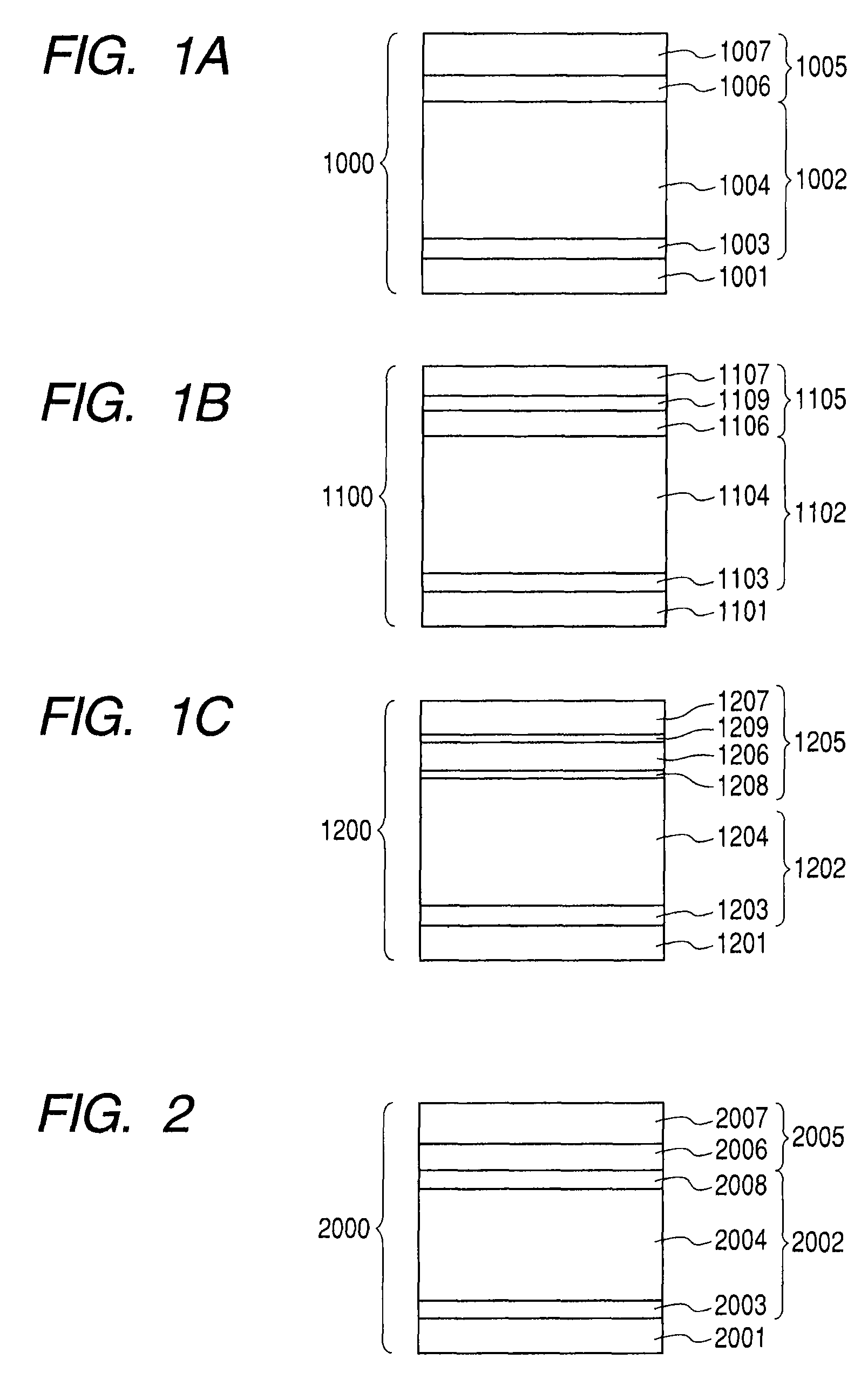
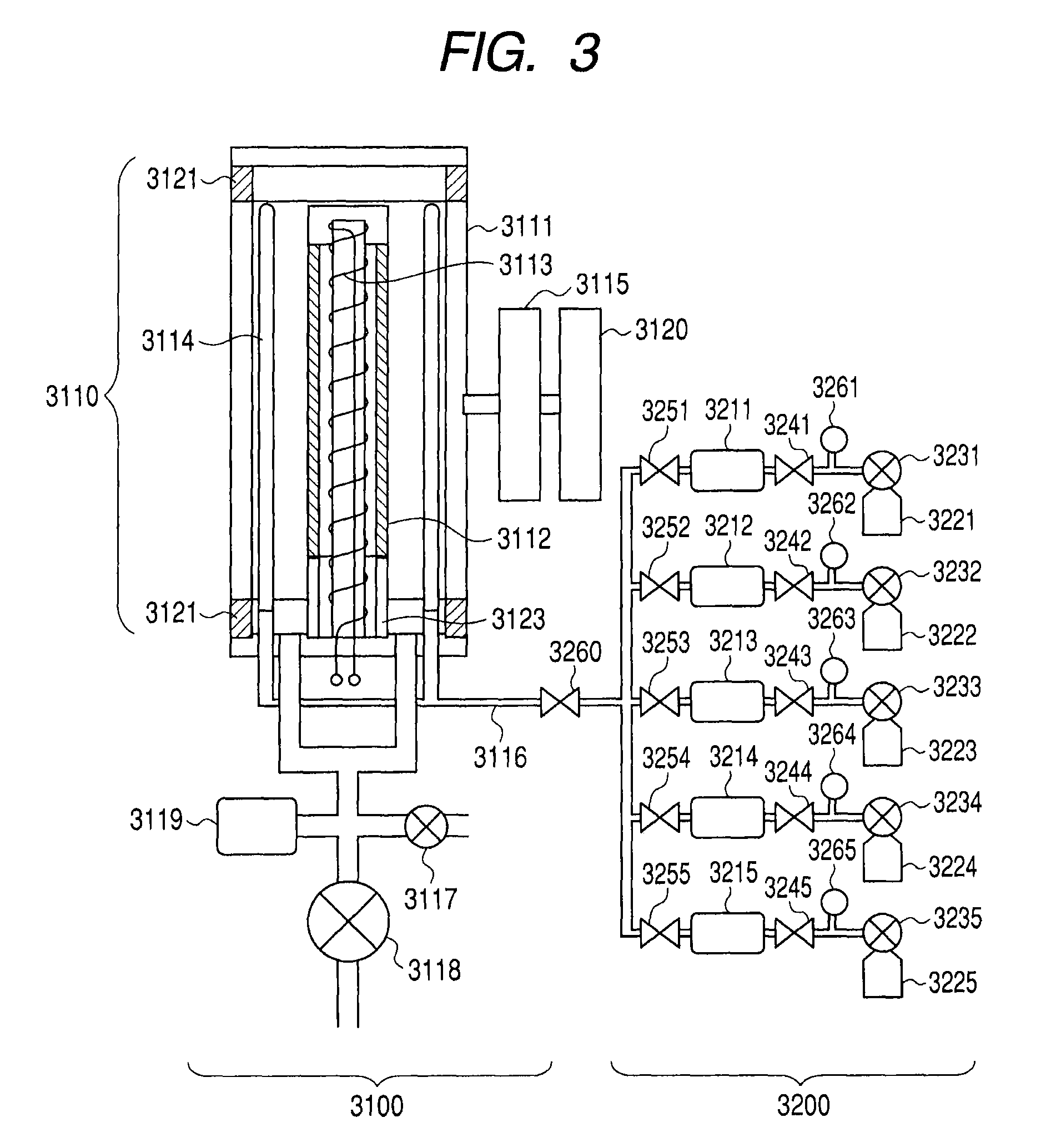
[0096]A positively chargeable a-Si photosensitive member was prepared by forming each layer on a conductive substrate (cylindrical substrate made from aluminum, which has diameter of 80 mm, length of 358 mm and thickness of 3 mm, and has been mirror-finished) by using a plasma treatment apparatus with the use of a high-frequency power source with an RF range as illustrated in FIG. 3, on conditions shown in the following Table 1 and Table 2. At this time, films of an electric-charge injection preventing layer, a photoconductive layer, a first surface layer and a second surface layer were formed (layer formation), in this order, and a film-forming period of time was controlled so that the film thicknesses of the layers could be respective values in Table 1. In addition, two electrophotographic photosensitive members were prepared for each film-forming condition.
[0097]
TABLE 1electric-chargeinjectionphoto-firstsecondpreventingconductivesurfacesurfacelayerlayerlayerlayergas type and flow...
example 2
[0147]Positively chargeable a-Si photosensitive members were prepared by forming each layer on the same conductive substrate as the above described one, by using a plasma treatment apparatus with the use of a high-frequency power source with an RF range as illustrated in FIG. 3, in conditions shown in the following Table 6 and Table 7. At this time, films of an electric-charge injection preventing layer, a photoconductive layer, a first surface layer and a second surface layer were formed (layer formation), in this order, and film-forming periods of time were controlled so that the film thicknesses of the layers could be respective values in Table 6. In addition, two electrophotographic photosensitive members were prepared for each film-forming condition.
[0148]
TABLE 6electric-chargeinjectionphoto-firstsecondpreventingconductivesurfacesurfacelayerlayerlayerlayergas type and flow rateSiH4 [mL / min (normal)]3504502525H2 [mL / min (normal)]7502200B2H6 [ppm ] (w.r.t. SiH4)15001NO [mL / min (n...
example 3
[0157]Positively chargeable a-Si photosensitive members were prepared by forming each layer on the same conductive substrate as the above described one, by using a plasma treatment apparatus with the use of a high-frequency power source illustrated in FIG. 3, which uses RF frequencies, in conditions shown in the following Table 10 and Table 11. At this time, films of an electric-charge injection preventing layer, a photoconductive layer, a first surface layer and a second surface layer were formed (layer formation) in this order, and a film-forming period of time was controlled so that the film thicknesses of the layers could be respective values in Table 10. In addition, two electrophotographic photosensitive members were prepared for each film-forming condition.
[0158]In the present example, a second joining layer is provided in between the first surface layer and the second surface layer. The electrophotographic photosensitive member (positively chargeable a-Si photosensitive memb...
PUM
 Abstract
Description
Claims
Application Information


